Photoluminescence
Absorption processes can be included to replicate photoresponse measurements. Device models can be constructed to simulate photovoltaics and photodetectors.
Note
A pre-made project file is available for this tutorial.
Create Materials
In this tutorial, we will model the photoluminescent behavior of an organic photovoltaic (OPV).
Donor
P3HT is used as the donor material. Excitation processes are assumed to be singlet-dominant. We therefore choose to use the Fluorescent Dye template.
We set a HOMO level of -5.2 eV and a LUMO level of -3.3 eV. For the excitons, we use a singlet binding energy of 1.2 eV and a triplet binding energy of 1.4 eV. Default Gaussian broadening is used for both polaron and exciton energy levels. The Dexter prefactor for excitonic transfer is set to 1.9.
The fluorescent material template will have automatically configured a radiative singlet decay process. We will set this rate to \(10^{7}\,\textrm{s}^{-1}\). We will simulate a singlet-mediated device by setting both singlet fractions to 1. ISC rates remain at zero.
Acceptor
PCBM is used as the acceptor material. We will use the Fluorescent Dye template to describe the singlet-dominant system.
We set a HOMO level of -6.1 eV and a LUMO level of -3.9 eV. For the excitons, we use a singlet binding energy of 1.6 eV and a triplet binding energy of 1.9 eV. Default Gaussian broadening is used for both polaron and exciton energy levels.
The Dexter prefactor for excitonic transfer is set to 3.1. The singlet radiative decay rate is set to \(10^{7}\,\textrm{s}^{-1}\). Both singlet fractions are set to 1.
Electron Transport Layer
BCP will be used as the electron transport layer. We select the Transport template to create a new material.
We set a HOMO level of -6.3 eV and a LUMO level of -2.9 eV. A Gaussian energy level broadening is enabled by default. For the excitons, we use a singlet binding energy of 1.5 eV and a triplet binding energy of 2.6 eV.
Hole Transport Layer
PEDOT:PSS will be used as the hole transport layer.
We set a HOMO level of -5 eV and a LUMO level of -2.3 eV. A Gaussian energy level broadening is enabled by default. For the excitons, we use a singlet binding energy of 0.7 eV and a triplet binding energy of 1.2 eV.
Create a Stack
We will utilize pure compositions to construct the OPV stack. We start with a 5 nm PEDOT:PSS hole transport layer. We then add 10 nm layers for both the P3HT donor and PCBM acceptor. A 5 nm BCP electron transport layer is added to complete the device.
Enable the automatic Förster processes option to include inter-layer singlet diffusion.
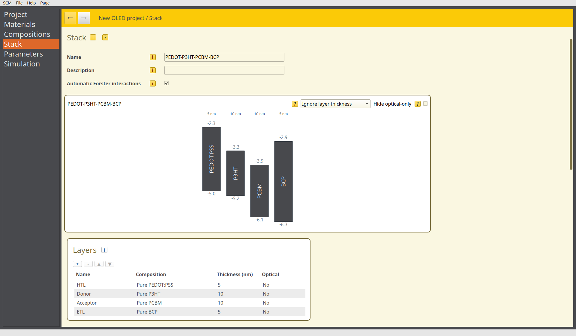
Fig. 84 OPV bilayer device in the stack editor
Photo-absorption processes can be added in the stack editor. Select the  button in the Absorption table to define a new absorption process. We select the P3HT material in the donor layer. Absorption is described as a fixed excitation probability per incident photon. We will assume a factor of 0.8, thereby accounting for a 20% loss due to optical processes. The singlet state is selected as the absorption product. We then repeat these steps to add the same reaction to the PCBM material in the acceptor layer.
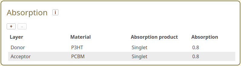
Fig. 85 Absorption configurations in the stack editor
Create a Parameter Set
Bumblebee offers multiple parameter templates for photoluminescent processes:
The Photoluminescence template configures a periodic system for measuring the bulk properties of the layer materials. In addition to configuring photo-absorption processes, higher resolutions are obtained compared to the default Bulk Simulation template
The Photovoltaic/Photodetector templates are used for regular (bipolar) device simulations
We will use the Photovoltaic template to model the photovoltaic device.
Device Settings
In the Main setting tab, we will set the electrode levels to -4.6 for a silver anode and -4.7 for an ITO cathode contact. The external device voltage will be set to 0.5 V.
Having chosen a PV template, the photoluminescence module should have been enabled automatically in the Modules tab.
Fluence
Photo-absorption settings are configured in the Photoluminescence tab.
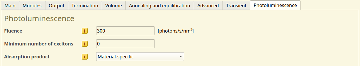
Fig. 86 Photoluminescence settings in the parameter set editor
The incident irradiation is set by defining a device fluence. We use a value of 300 photons/s/nm\(^3\), in line with ambient solar lighting conditions.
The absorption product is configured to be material-specific by default. This will use the absorption products defined earlier in the Stack editor. This selection can also be overwritten to force a specific absorption product for the whole device. We can keep the default value during this tutorial.
When simulating bulk material properties, a minimum exciton density can also be added in this tab. For the current device simulation, we will keep this value at 0.
Starting the Simulation
For this tutorial, we will set up a new simulation using a single trajectory instance.
A fluence sweep can be performed to investigate how the device current changes as a function of the irradiation. We choose to vary the fluence from 300 to 1500 photons/s/nm\(^3\) in 5 steps.
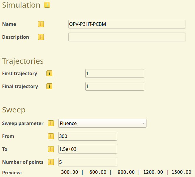
Fig. 87 Fluence sweep setup in the simulation settings
Once you are done, use File → Save and File → Run to start the simulation.
Tip
If you wish to limit the computational time required for this tutorial, you can perform a single-point calculation (Sweep → None) instead. This will use the 300 photons/s/nm\(^3\) default fluence defined in the parameter set.
Simulation Output
We can view the transient photoluminescence rate from the Sweep → Photoluminescence → Transient Luminescent Decay Rate section of BBresults. As the simulation progresses, the rate of luminescence is seen to stabilize, with the steady-state singlet density equilibrating absorption, emission and quenching processes.
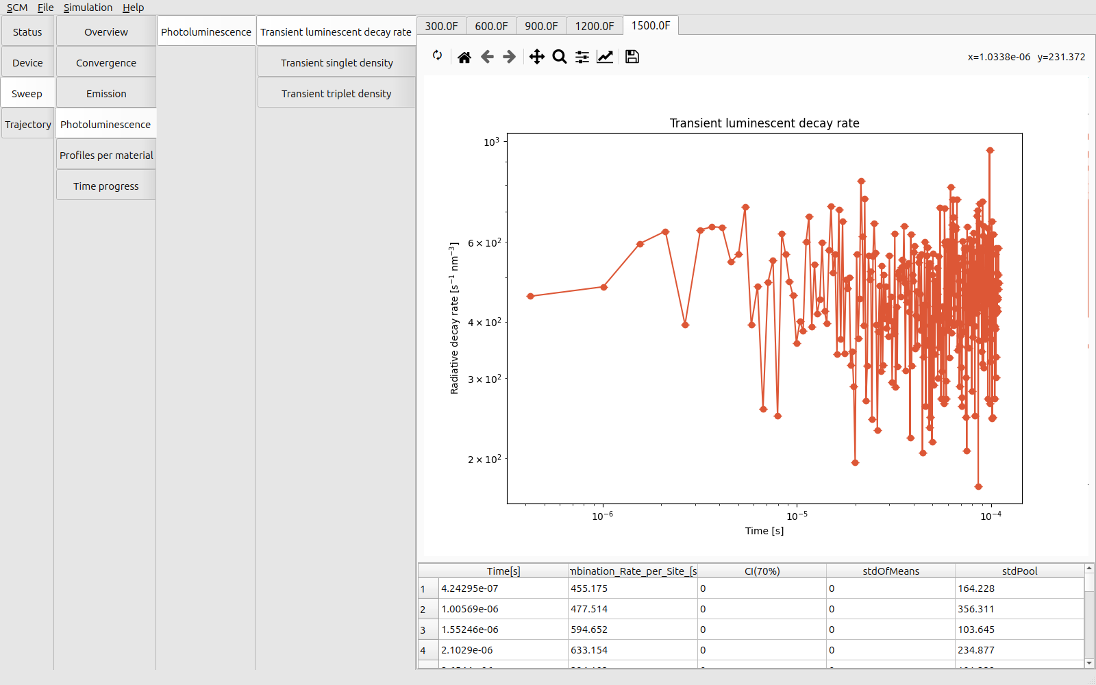
Fig. 88 Transient singlet luminescence at an incident fluence of 1500 photons/s/nm\(^3\)
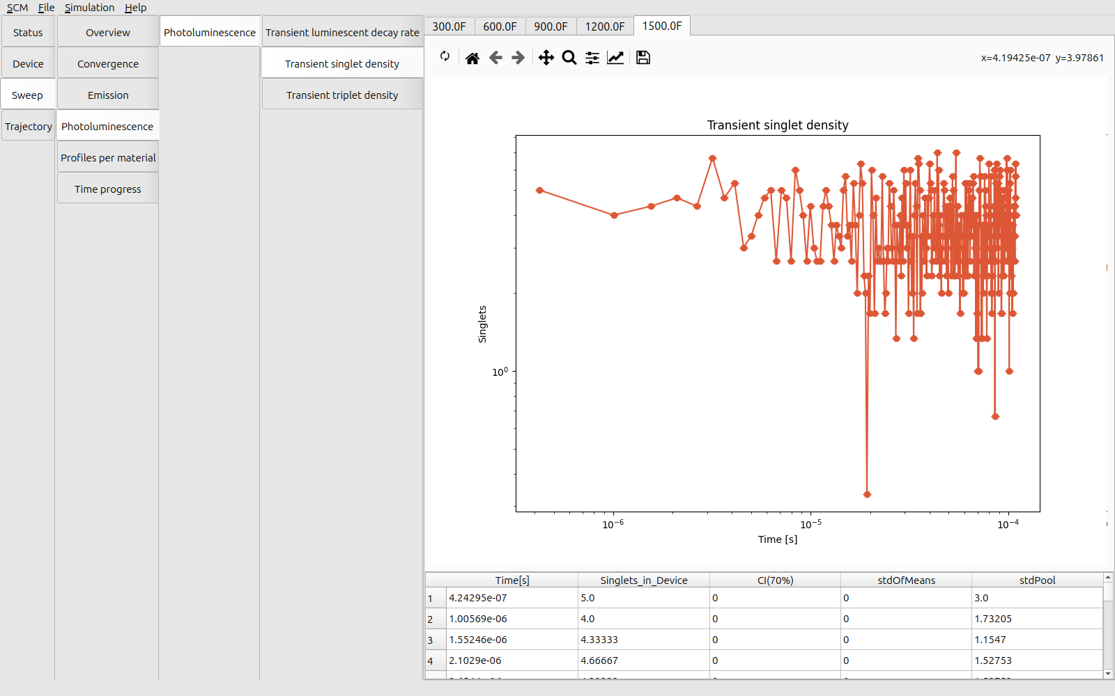
Fig. 89 Transient singlet density at an incident fluence of 1500 photons/s/nm\(^3\)
Singlets are generated uniformly in the center of the device, in line with the dictated absorption processes. The distributions can be found under Sweep → Profiles per Material → Occupations. A slight depression is noted at the interface between the donor and acceptor layers. Charge separation occurs at the interface, resulting in a higher quenching rate (Sweep → Profiles per Material → Rates → Quenching Rate) and thus a lower local concentration of excitons.
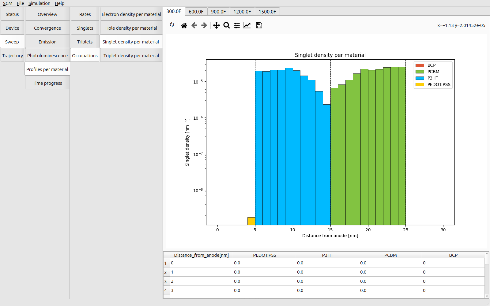
Fig. 90 Steady-state singlet distribution at an incident fluence of 300 photons/s/nm\(^3\)
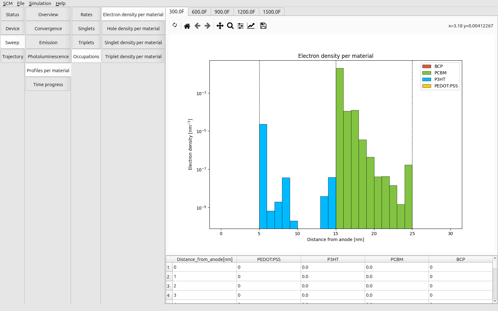
Fig. 91 Steady-state electron distribution at an incident fluence of 300 photons/s/nm\(^3\)
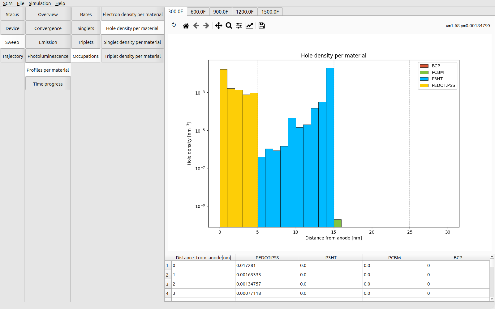
Fig. 92 Steady-state hole distribution at an incident fluence of 300 photons/s/nm\(^3\)
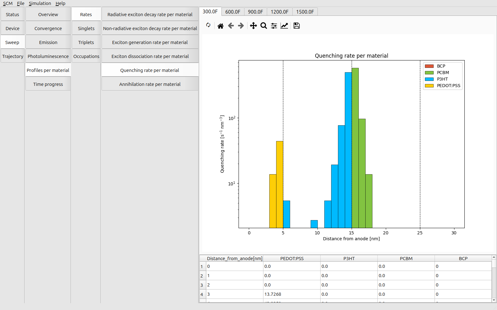
Fig. 93 Steady-state quenching rates at an incident fluence of 300 photons/s/nm\(^3\)
With an increased fluence, the singlet density and luminescent emission rates are seen to increase. This is reflected in the internal electrostatic field gradient, which increases in proportion to the free carrier density.
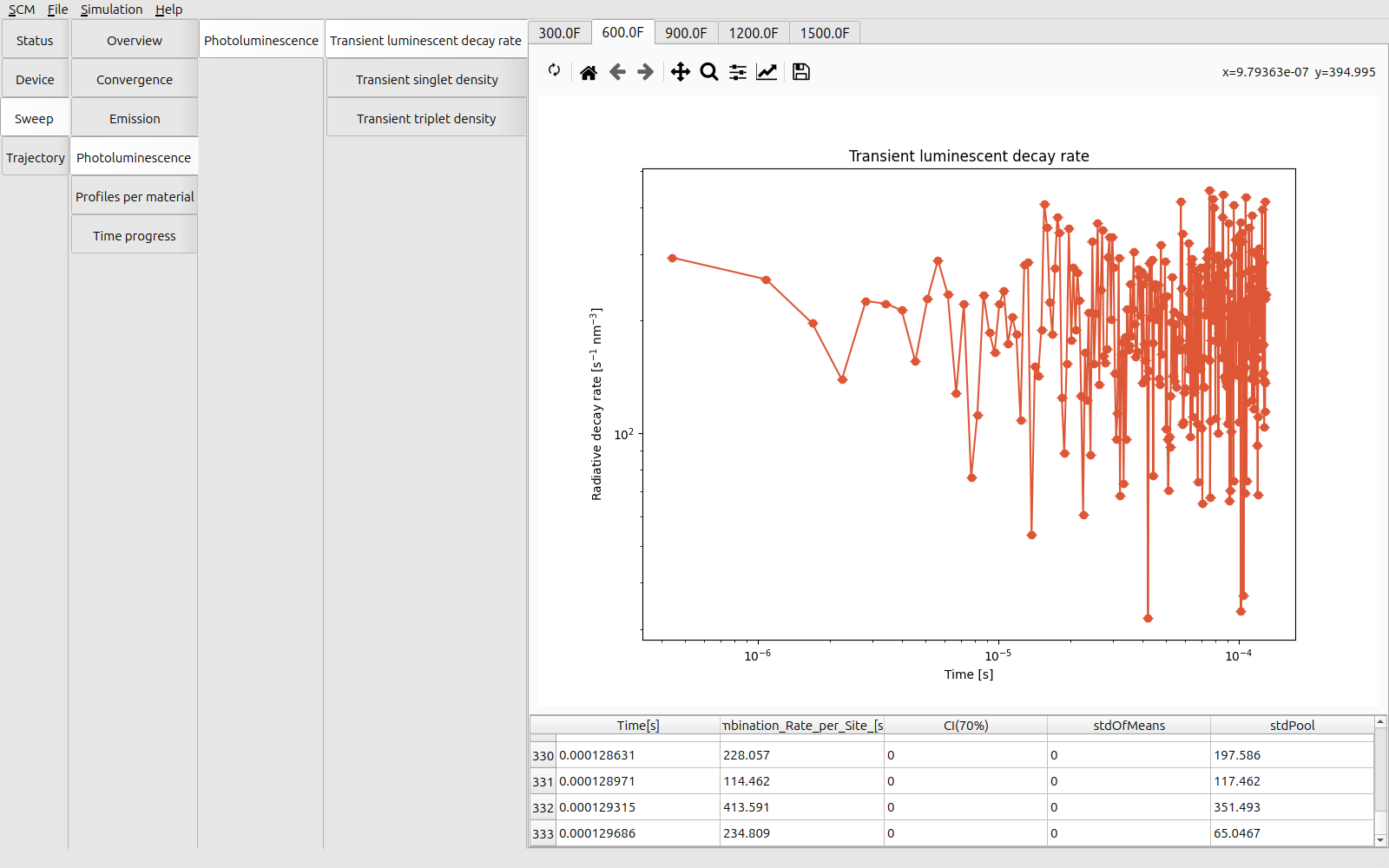
Fig. 94 Transient singlet luminescence at an incident fluence of 600 photons/s/nm\(^3\)
The objective of this tutorial was to monitor the steady-state PL response of an OPV device. If we wanted to model the photocurrent generation process, we would run the simulation at a higher voltage to achieve faster separation of charges. A voltage sweep can then be employed to determine the \(V_{\textrm{OC}}\), \(J_{\textrm{DC}}\) and fill factor.
See also
For dynamic PL measurements, one would not use a constant illumination intensity. Pulsed illumination is commonly used to inject excitons into the OPV device, before subsequently monitoring JV and re-emission profiles to characterize device efficiencies. These pulsed illumination experiments can be replicated using the pulse or checkpoint settings found in the Transient tab of the Parameters page.
Check out the transient response tutorial for more details.
See also
We have configured a uniform generation of excitons over the dual-layer device. A bulk heterojunction morphology could also be created through the use of Advanced Compositions. This would provide a more realistic picture of charge distribution between donor and acceptor species at the interface.
Consult the morphology tutorial for more details.