
Thermally Activated Delayed Fluorescence (TADF)
Thermally activated delayed fluorescence (TADF) emitters are known for achieving high device efficiencies. In first-generation fluorescent emitters, only singlet excitons undergo radiative decay, leaving triplet excitons unused. Because 75% of the generated excitons are triplets, according to spin statistics, this results in a significant loss of efficiency. In TADF emitters, the energy gap between the first excited singlet state (S1) and the first excited triplet state (T1) is sufficiently small to enable reverse intersystem crossing (RISC) through thermal activation. As a result, triplet excitons are converted into singlet excitons, which can then undergo the spin-allowed radiative S1 → S0 transition. Through the RISC process, a much larger fraction of the generated excitons can undergo radiative decay, making TADF emitters significantly more efficient than first-generation fluorescent emitters.
In this tutorial, we will model a single-layer TADF device presented by Kotadiya et al. [1] We will showcase how Bumblebee can be used to determine the mobility parameters of the device in order to analyze the photophysics.
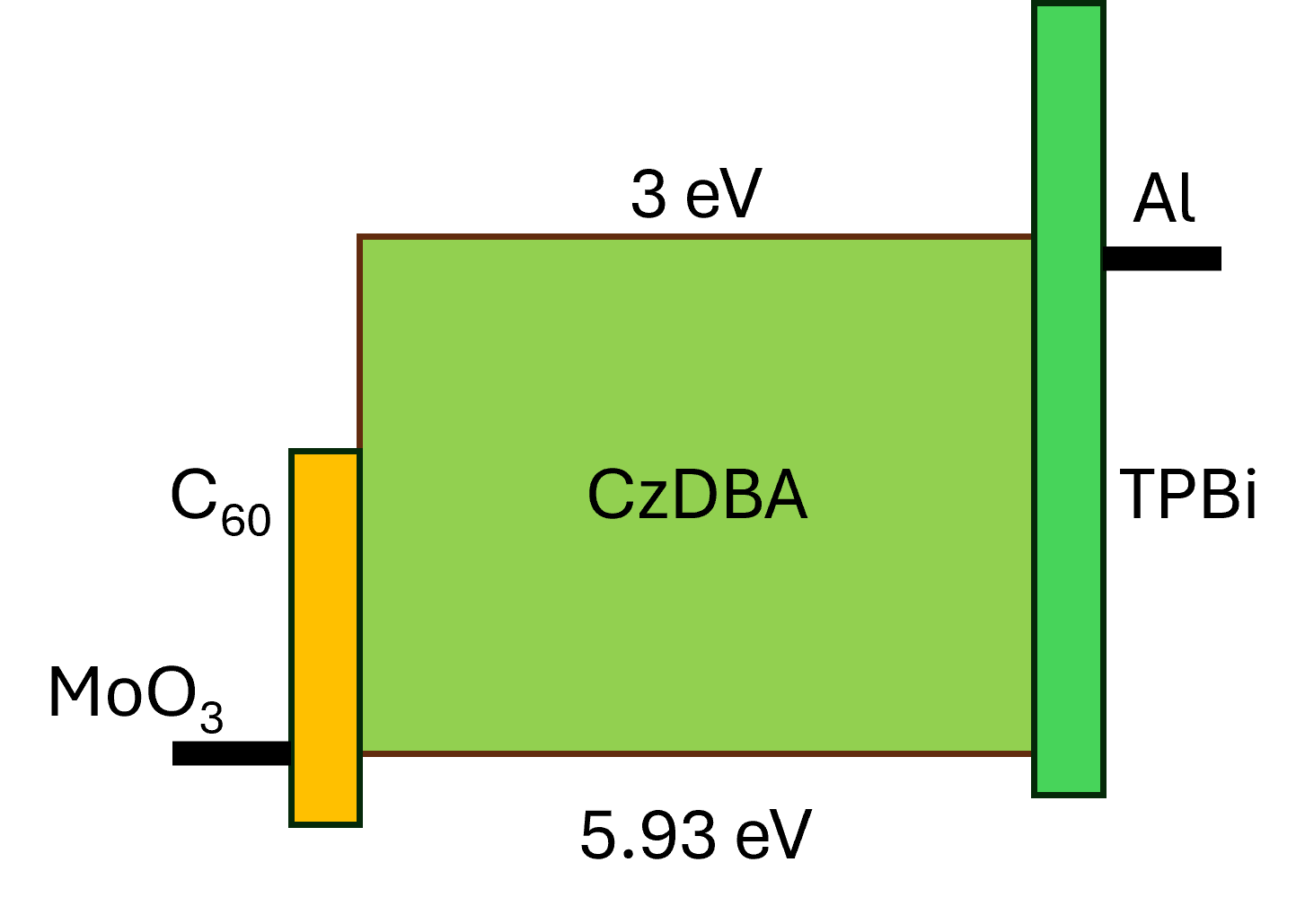
Fig. 128 Single-layer TADF OLED device.
Note
A pre-made project file is available for this tutorial.
Create Materials
We only require to create the TADF emitter material. Open an empty project in BBinput, then move to the materials tab. Create a new material with the TADF dye material template. Adjust the following input parameters:
- Electronic
HOMO = -5.93 eV
LUMO = -3 eV
- Excitonic
Singlet binding energy = 2.21 eV
Triplet binding energy = 2.17 eV
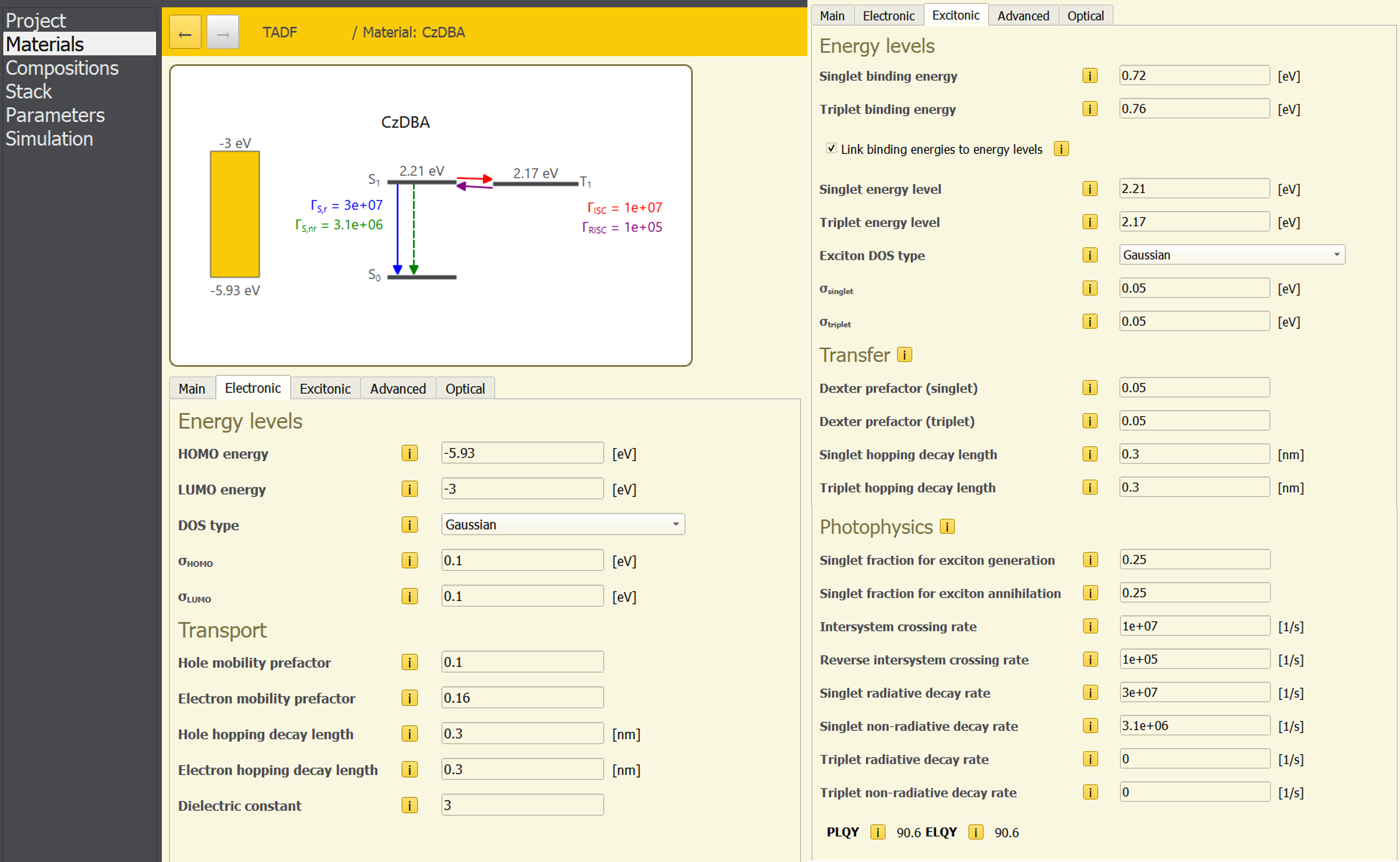
Fig. 129 CzDBA input parameters.
The HOMO and exciton energy levels are taken from the paper of Kotadiya et al. [1] The singlet and triplet energy levels are determined by taking the maximum of the emission spectrum reported in the paper (560 nm), which results in a singlet energy level of 2.21 eV. A singlet-triplet gap of 0.04 eV was reported by Wu et al. [2], which is used to set the triplet energy level to 2.17 eV. The LUMO value entered into Bumblebee is 0.5 eV higher compared to the CV-measured value to account for the adiabatic relaxation.
The (reverse) intersystem crossing rate and the PLQY reported by Wu et al. [2] are entered in the Photophysics section. The singlet radiative decay rate is obtained from the reported lifetime. The non-radiative decay rate was determined from the radiative decay rate and the PLQY.
- Photophysics
Intersystem crossing rate = \(10^{7}\,\textrm{s}^{-1}\)
Reverse intersystem crossing rate = \(10^{5}\,\textrm{s}^{-1}\)
Triplet radiative decay rate = \(3\cdot{}10^{7}\,\textrm{s}^{-1}\)
Triplet non-radiative decay rate = \(3.1\cdot{}10^{6}\,\textrm{s}^{-1}\)
The PLQY reported by BBinput should now read as 90.6%.
All other parameters are left at their default settings. Click the Save Material button at the top of the page to save the material input.
Create the Stack
Under the Stack tab, add a single layer of CzDBA with a thickness of 75 nm in the Layers table.
Scroll down to the Förster interactions tab and click the Add default interactions button to include the relevant excitonic processes. Set the Förster radii for Triplet diffusion and Singlet diffusion to 1.5 nm. The remaining Förster radii are set to 2 nm.
Save the stack at the top of the page with the Save stack button.
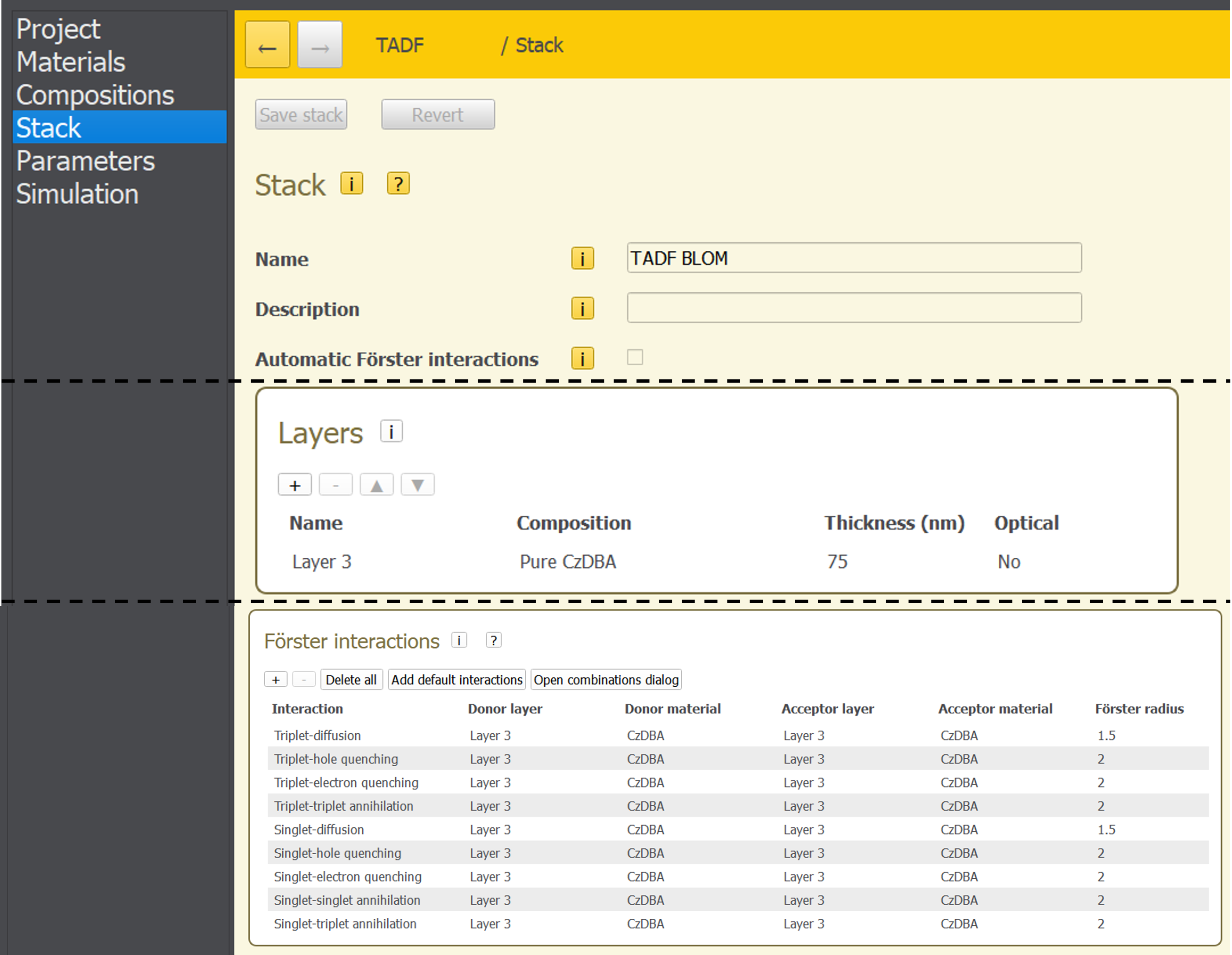
Fig. 130 Stack input parameters.
Create a Parameter Set
Navigate to the Parameters tab to set the simulation parameters. Load the preset Voltage sweep (bipolar) settings. The contacts described in the reference paper are Ohmic contacts, which are configured automatically by BBinput. The C60 and TPBi layers are modeled implicitly as they are considered part of the Ohmic contacts. [1] A convergence threshold of 0.05 can be set under the Termination tab to automatically terminate the simulation once the JV data has converged. All other parameter settings are left at their default values.
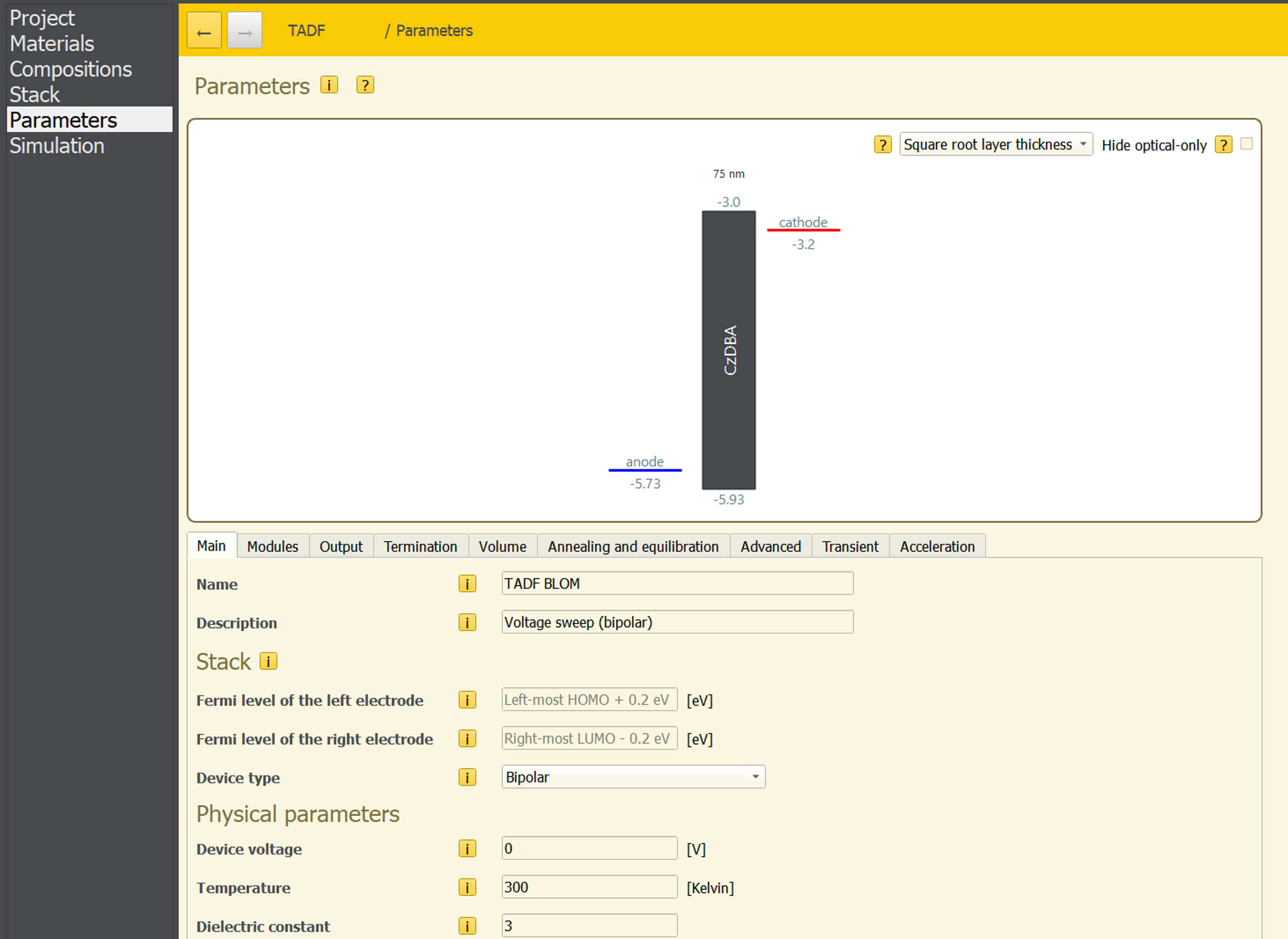
Fig. 131 The final stack, including contacts.
Start the Simulation
The voltage sweep range is set in the Simulation tab. For this tutorial we set the following values:
- Trajectories
First trajectory = 0
Final trajectory = 3
- Sweep
Sweep parameter = voltage
From = 2
To = 5
Number of points = 7
After setting the parameters, save the simulation input for using File → Save. Use File → Run to start the simulation.
Parameter Fitting
In order to reproduce the experimental JVL behavior of the experimental device, we will fit the mobility parameters of the single-layer device. Both the charge and exciton mobilities will be considered.
As a starting point, we use the hole/electron mobility ratio based on experimental TOF. [1]. (Though these values will need to be adjusted later to correct for finite field effects in the measurement.) The exciton mobilities are assumed to be half the electron and hole mobilities, reflecting the fact that an exciton is a bound electron-hole pair and is therefore expected to be less mobile than the individual charge carriers. Results for various mobility values are summarized below:
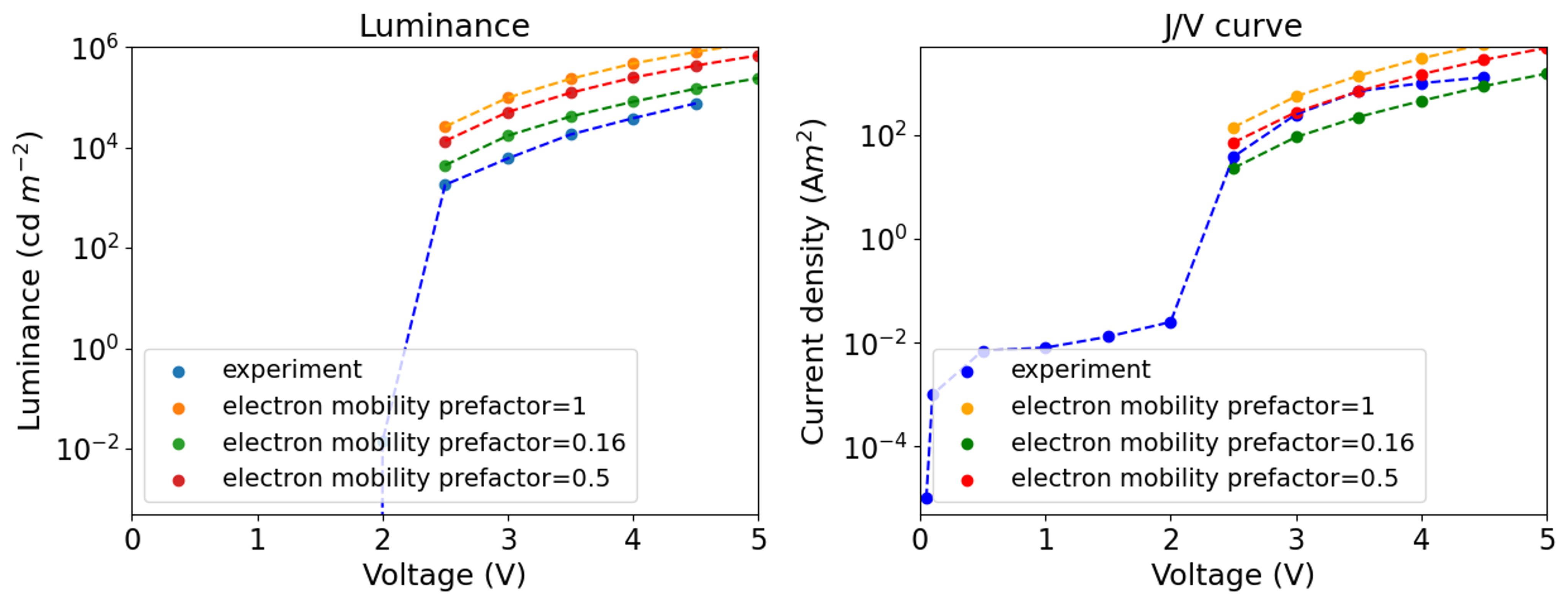
Fig. 132 Luminance-voltage and current-voltage curves for different mobility settings.
The difference in the J/V curves shows that for an electron mobility prefactor of 1, the current density is systematically too high. An electron mobility prefactor of 0.5 provides better agreement with the experimental data. However, comparison with the experimentally measured luminance shows that this mobility value still overestimates the experimental results. Based on both current density and luminance compatibility, the electron mobility prefactor is set to 0.16 for the final simulations.
After device optimization, the final parameters used for the mobilities of CzDBA are the following:
- Electronic
Hole mobility prefactor = 0.1
Electron mobility prefactor = 0.16
- Excitonic
Dexter prefactor (singlet) = 0.05
Dexter prefactor (triplet) = 0.05
The mobilities can be changed under the Materials tab. Select CzDBA and click on the pencil icon to return to the parameter input page. Adjust the mobilities and click the Save material button at the top of the Materials page to save the adjustments to the material. Subsequent simulations will now be run using the fitted mobilities.
Simulation Output
The simulation results can be viewed using BBresults.
External Quantum Efficiency (EQE):
In BBresults, the calculated EQE can be viewed under the tab Overview → EQE. A comparison between the experimental and simulated EQE is provided here:
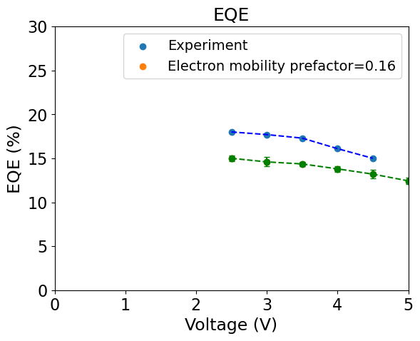
Fig. 133 Comparison of experimental and simulated EQE at each voltage.
The simulated EQE is in good agreement with the experimental results. Residual errors are attributed to a difference in the outcoupling efficiency used by BBresults (20%) and that of the experimental device (ca. 23%).
Tip
Enabling the Optical module in the Parameters → Modules tab will perform an optical outcoupling calculation on the device. The calculated outcoupling will then be used automatically by BBresults, reducing the EQE discrepancies. Note however, that this requires full specification of the device optics, which has been omitted here for brevity.
Event distribution:
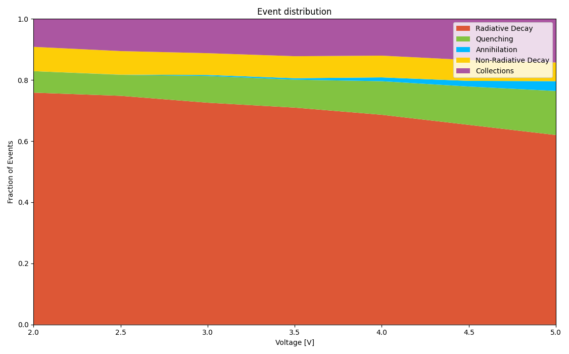
Fig. 134 Event distribution obtained by Bumblebee (BBresults: Device → Overview → Performance → Event distribution).
The event distribution gives an insight into the processes happening in the device. As expected from the high IQE, radiative decay is the dominant process in the device. As voltage is increased, the radiative decay declines and contributions from annihilation, and quenching losses grow.
The event distribution shows a substantial fraction of collections. Collections are charge carriers that have moved to the opposing electrode. For a single-layer device, the occurrence of collections is to be expected, as there are no additional layers to shield the electrodes. The number of collections increases with increasing voltage, primarily due to exciton dissociation, making it more likely that an exciton does not participate in radiative decay. This increases the amount of free charge carriers in the system, making collections more likely.
Emission spectra:
The emission spectrum shows peaks that closely match the experimental data. This is expected, as the singlet energy level input is based on the wavelength corresponding to the maximum intensity of the PL peak. The width of the peak is tied to the Gaussian energy level distribution provided on the Materials page, providing reasonable agreement with the experimentally measured peak broadening.
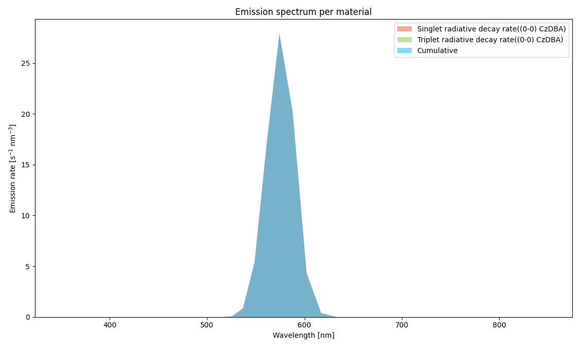
Fig. 135 Simulated emission spectra at 5V (BBresults: Sweep → Emission → Emission spectrum per material → 5V).