Exciton Simulation
The basic working of an OLED is to excite molecules with a current. The desired effect is that the molecules return to the ground state via radiation. Therefore excitonics are the heart of the OLED. In this tutorial we show some design principles and calculate the luminance and efficiency of the proposed OLED.
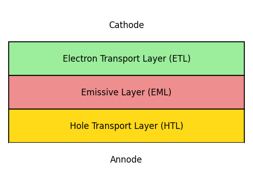
Fig. 35 The stack has three layers, abbreviated as HTL/EML/ETL. Here the layout is vertical, but in BBinput a horizontal layout is used, i.e. the above picture rotated clockwise by 90 degrees.
In this tutorial, a phosphorescent emitter is considered. Loss processes are included using both Dexter (short range) and Förster (long range ) mechanisms.
Open BBinput and set the project name to Exciton Simulation.
Note
Entering correctly the parameters can be a daunting task. You may prefer to download the project file
Create Materials
To construct the OLED device stack, we will create an electron transport layer (ETL), a hole transport layer (HTL) and a host-guest emissive layer (EML). This requires the definition of 4 materials.
Tip
If you have never created materials before, take a look at the start of the bulk tutorial.
Phosphorescent Dye
Ir(ppy)3 is used as the phosphorescent dye. We will select the corresponding template when creating a new material on the Materials page.
On the Electronic tab, we specify a HOMO level of -5.27 eV and a LUMO level of -1.86 eV. A Gaussian broadening is enabled by default.
Several material-specific parameters are specified to describe exciton generation and emission. These parameters are set on the Excitonic tab of the material editor.
We will set a singlet binding energy of 0.75 eV and a triplet binding energy of 1 eV. By enabling the option to link the singlet and triplet binding energies, the exciton energy levels will be computed automatically based on the exciton binding energy and the HOMO/LUMO levels.
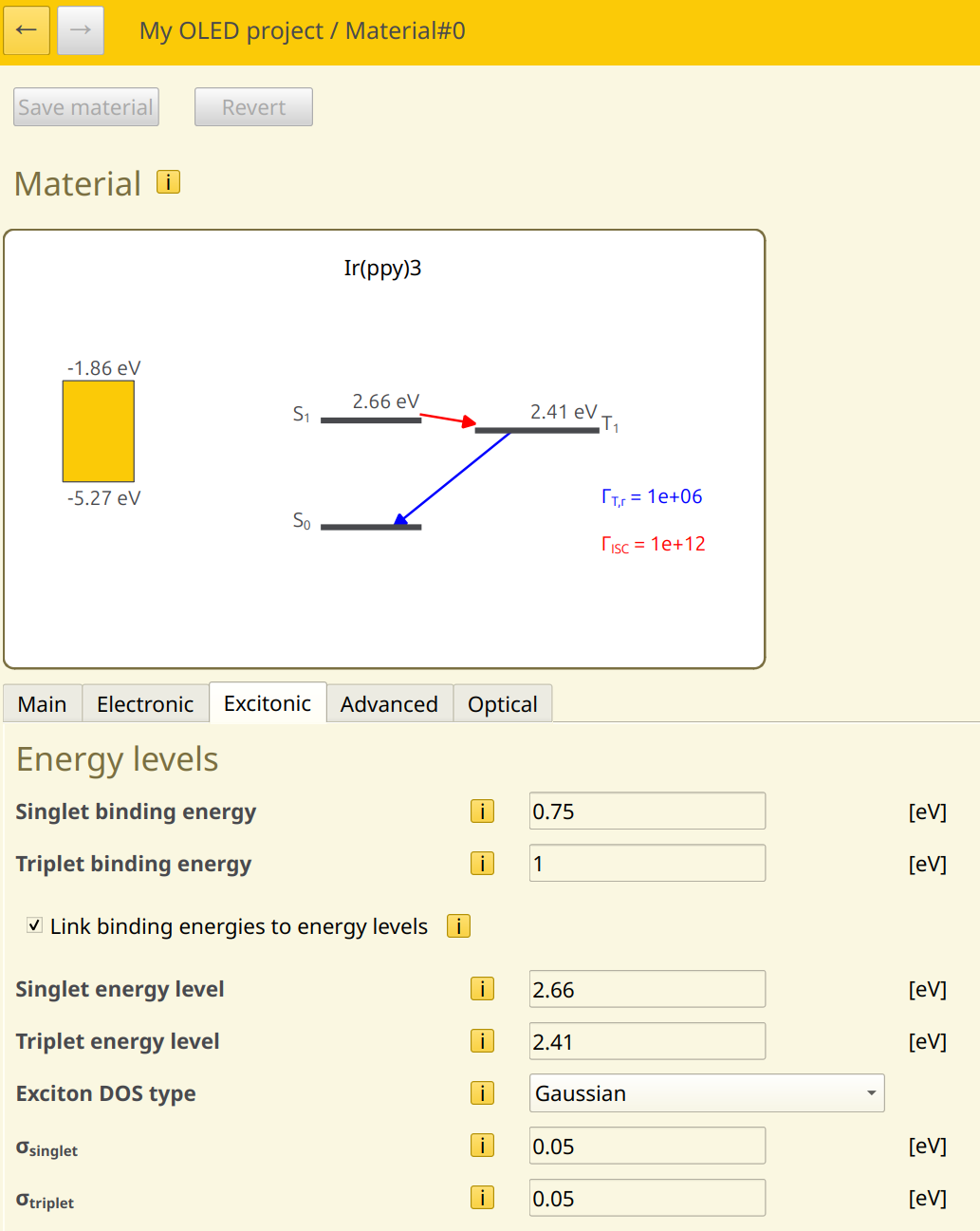
Fig. 36 Exciton binding energies and energy levels can be linked automatically
An energy level broadening is defined for the exciton levels, just as we did for the polaron levels, accounting for the variations in molecular parameters due to the inhomogeneous environment of the layer. A Gaussian broadening is used, this time with a width of 0.05 eV.
To describe Dexter-type exciton diffusion, Dexter transfer parameters are specified. We choose a prefactor of 1, with a decay length of 0.3 nm.
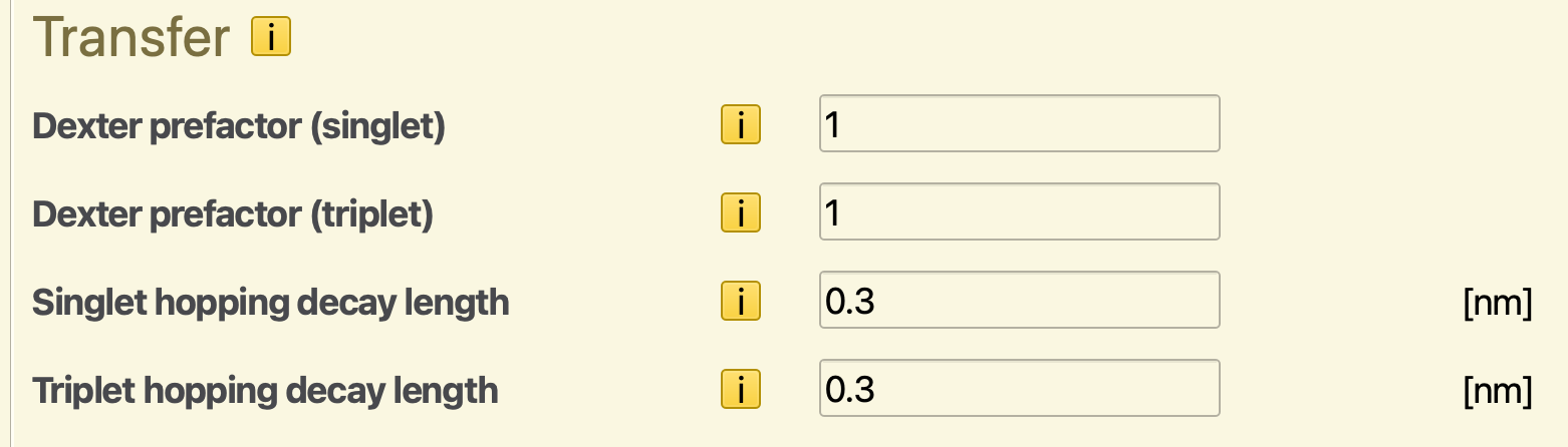
Fig. 37 Rate constants for Dexter-type exciton transfer
Note
The rates of transfer processes is specified in normalized units. I.e. the true prefactor is multiplied by a normalization factor. This time unit is specified in the parameter set.
This decomposition allows us to write the material parameters using convenient factors.
In contrast, the radiative processes are provided in natural units, without normalization. These parameters specify the real frequency in the input, with normalization applied internally by Bumblebee.
By selecting the phosphorescent material template, the singlet fractions will have been set to 0, such that the exciton generation products will exclusively be triplets.
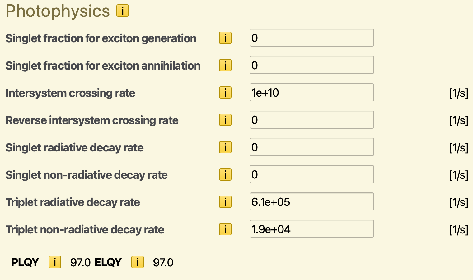
Fig. 38 Förster prefactors, intersystem crossing frequencies and singlet-triplet distributions. The PLQY and ELQY are reported automatically based on the provided rates
An intersystem crossing rate of \(10^{10}\,\textrm{s}^{-1}\) will be specified. The reverse intersystem crossing rate is set to 0. This allows any singlets obtained through e.g. exciton transport to be irreversibly converted to triplets.
The radiative decay rate of the triplet excitons is set to \(6.1\cdot{}10^{5}\,\textrm{s}^{-1}\). The non-radiative decay rate is set to \(1.9\cdot{}10^{4}\,\textrm{s}^{-1}\). The photoluminescent and electroluminescent quantum yields of the dye are now reported to provide an indication of the molecular emitter efficiency.
Note
Förster processes will be configured in the stack editor. Because Förster transfer describes a dipolar process, the rate parameters exhibit strong variations with molecular environment. The stack editor allows definition of custom rates for inter-layer transfer processes, and allows definition of multiple intra-layer Förster processes to account for more complex rate expressions.
Host
CBP is used as a host material. Select the appropriate template when creating a new material entry.
We use a HOMO level of -6.08 eV and a LUMO level of -1.75 eV. A Gaussian broadening is enabled by default. For the excitons, we use a singlet binding energy of 1 eV and a triplet binding energy of 1.7 eV. For Dexter-type exciton transfer, a prefactor of 0.95 is used along with a decay length of 0.3.
The singlet-triplet generation ratio will be set to 0.25 (corresponding to a statistical 1:3 distribution of singlet and triplet excitons).
Thermalization losses during exciton transport from the dye through the host are included by setting the non-radiative decay rates to \(10^{5}\,\textrm{s}^{-1}\) for singlets and \(10^{4}\,\textrm{s}^{-1}\) for triplets. The radiative decay rates are set to 0.
Electron Transport Layer
TPBi is used as an electron transport layer. Select the Transport layer when creating a new material.
We use a HOMO level of -6.2 eV and a LUMO level of -1.7 eV. For the excitons, we use a singlet binding energy of 0.75 eV and a triplet binding energy of 1 eV. For Dexter-type exciton transfer, a prefactor of 1 is used along with a decay length of 0.3.
To mimic the effect of an exciton diffusion barrier in the stack, a non-radiative decay rate of \(10^{8}\,\textrm{s}^{-1}\) is specified for both excitons.
Hole Transport Layer
TAPC is used as the hole transport layer. We use a HOMO level of -5.5 eV and a LUMO level of -0.96 eV. For the excitons, we use a singlet binding energy of 1 eV and a triplet binding energy of 1.59 eV. For Dexter-type exciton transfer, a prefactor of 1 is used along with a decay length of 0.3. A non-radiative decay rate of \(10^{8}\,\textrm{s}^{-1}\) is specified for both excitons.
Create Compositions
We will create a host-guest mixture containing 0.9 CBP and 0.1 Ir(ppy)3.
Create a Stack
We start by composing the stack layers. We use a 20 nm TAPC hole transport layer, a 30 nm host-guest layer in the center and a 20 nm TPBi electron transport layer.
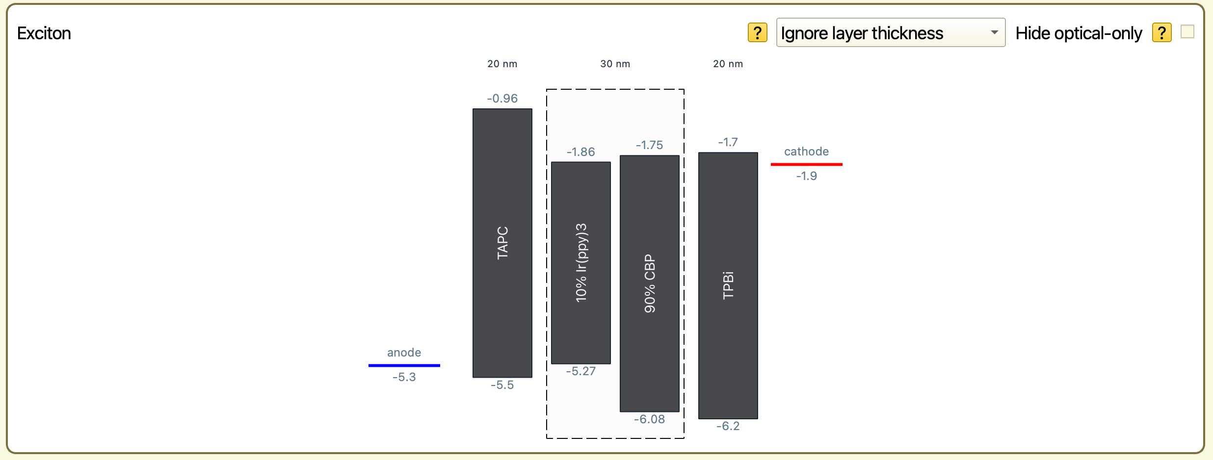
Fig. 39 The three layers HTL/EML/ETL. Why could this make a good OLED? The holes will go from left to right and for those you need to look at the HOMO levels, i.e. the bottom of the blocks. Holes can go from the HTL to the emissive layer when the target HOMO is higher. This is true for the 10% phosphorescent material, but not for the 90% CBP host. Holes cannot pass from the EML to the ETL, as the latter has a lower HOMO. For electrons to cross a layer boundary the target LUMO (top of the block) needs to be lower. In going from the ETL to the EML this is true for both compounds in the EML. Based on this simplified argumentation we expect: 1) a slower penetration of holes from the HTL to the EML, and no penetration of holes to the ETL. 2) Fast penetration of electrons from the ETL to the EML, but no further penetration into the HTL. This design ensures that there can only be both electron and holes in the EML where they can combine to make excitations. If these decay with radiation there is light.
The stack editor now allows us to define the Förster radii. Förster rates are defined for various processes, including diffusion, quenching and annihilation. Because the Förster rates depend on the molecular environment, separate reactions have to be specified for each pair of materials. To streamline this process, the GUI provides the option to automatically configure the most common processes for the current stack. The mechanisms that are included are based on the material templates.
Enable the Auto Förster option. This will include the triplet diffusion, triplet quenching and exciton annihilation reactions.
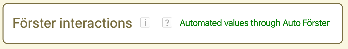
Fig. 40 When using Auto Förster, the corresponding table is disabled.
Create a Parameter Set
Press the Load preset button on the Parameters page and select the Single voltage point template. In the Main tab, we set the default device voltage to 5 V. In the Termination tab, the maximum number of simulation steps is set to 1,000,000,000.
Because carrier mobilities are enhanced at higher voltages, the required number of steps typically changes during a voltage sweep. To account for this, we can have the simulation terminate automatically a stable current has been reached. On the Termination tab, we set a convergence threshold of 0.1. This will automatically stop the simulation once the current is uniform over 90% of the device.
Excitonic processes are included in the simulation by enabling the excitonics module. The single voltage point template includes this option by default. You can check the module configuration by navigating to the Modules tab.
Starting the Simulation
A voltage sweep can be performed to investigate the roll-off in device efficiency at higher voltages. We select a voltage range from 3 to 6 V and select 7 voltage points. A single disorder instance can be selected to decrease the simulation runtime.
If you wish to limit the computational time required for this tutorial, you can perform the single voltage point simulation instead. This will use the 5 V default chosen in the parameter set.
Simulation Output
We can use BBresults to analyze the output of our simulation (SCM → BBresults). BBresults can also be used to monitor ongoing simulations, so we can see how the statistics evolve as time progresses.
The distribution of electrons and holes over the stack layers can be viewed in the Device → Profiles section.
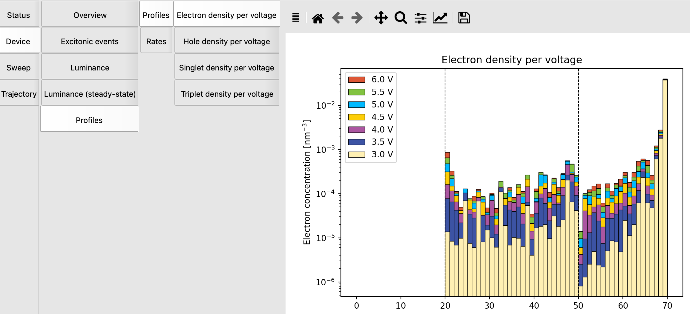
Fig. 41 Voltage-dependent electron density in the OLED stack
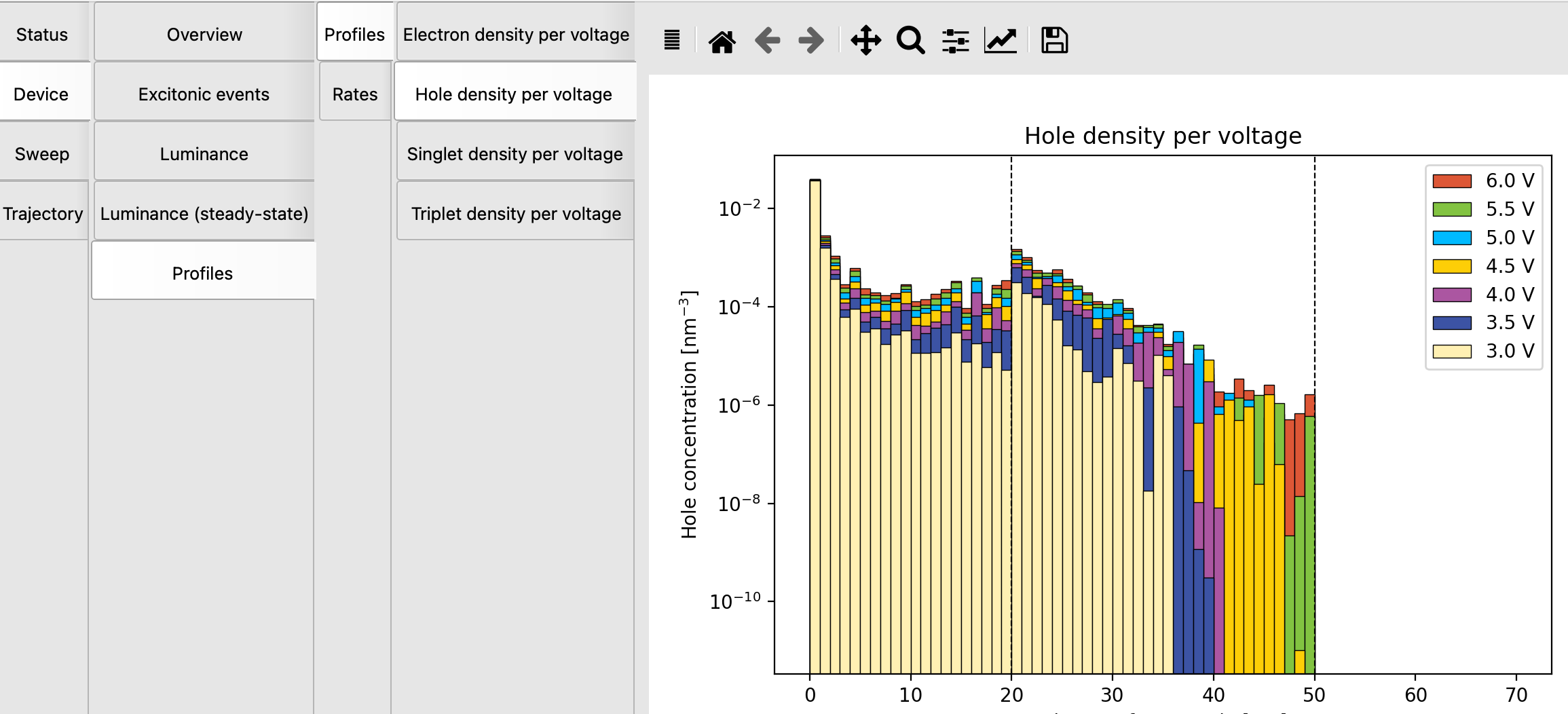
Fig. 42 Voltage-dependent hole density in the OLED stack
A good sign is that there are (almost) no electrons in the HTL and no holes in the ETL: we want them to only combine in the emissive layer. The graphs show that no hole or electron blocking layers are needed.
Because we are using a phosphorescent emitter, the triplet distribution is a key indicator for the quantum yield.
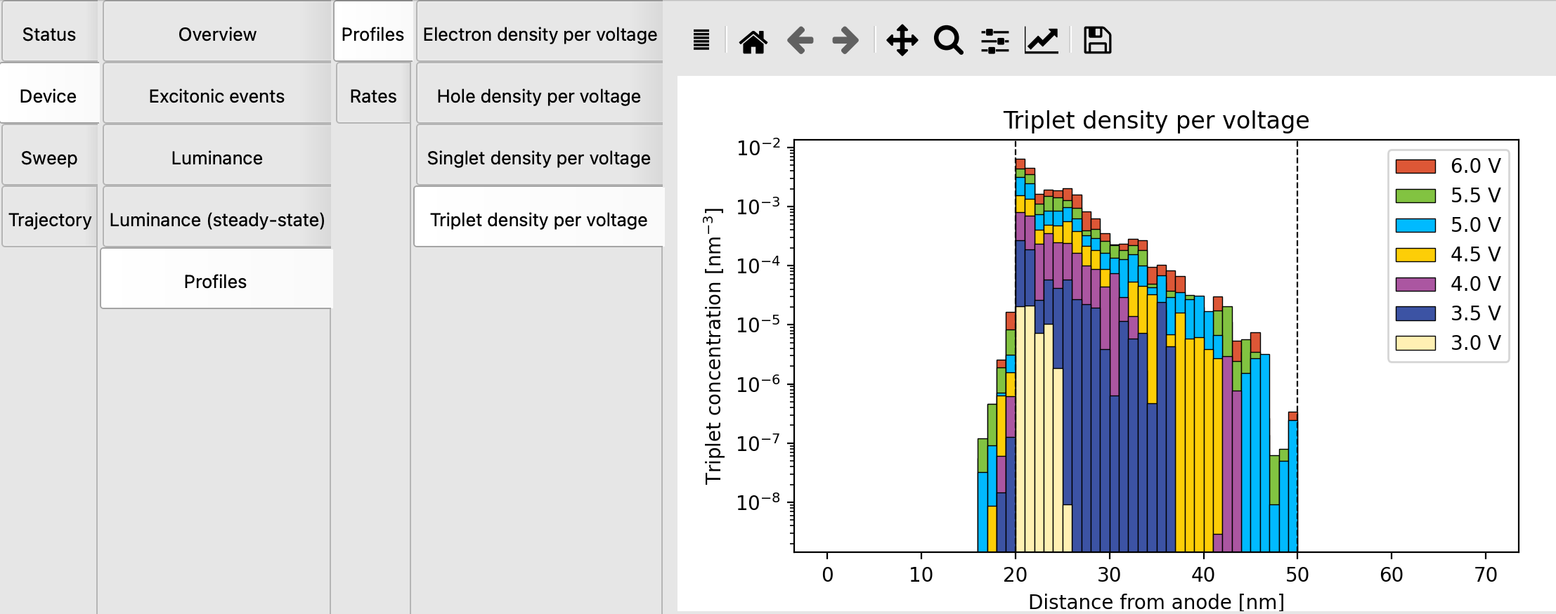
Fig. 43 Voltage-dependent triplet density in the OLED stack. Clearly most are generated on the left of the EML (mind the log scale). This is consistent with the idea that holes penetrate the EML from the left more slowly than electrons from the right. There is some “leakage” into the HTL, due to Förster triplet diffusion.
Triplets are primarily located at the HTL/EML interface, with hole injection appearing to limit the exciton density.
Device losses can be analyzed in the Device → Overview → Performance → Event Distribution. The desired process is radiative decay, with other processes reducing the OLED efficiency through a decrease in the exciton density.
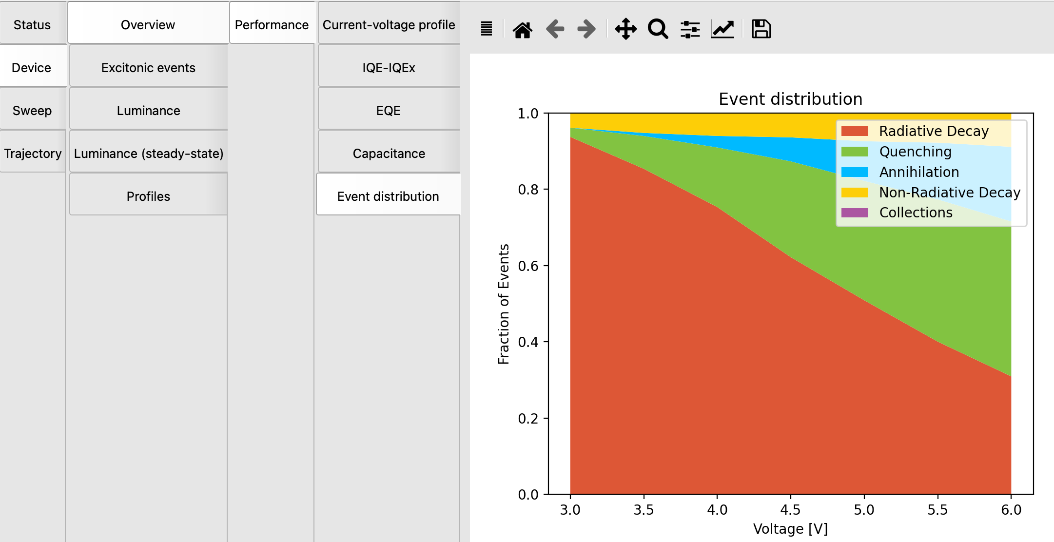
Fig. 44 Distribution of processes as a function of voltage. At higher voltages there is rather a lot of quenching going on, suppressing the radiative decay.
Finally you can consider the important trade-off between luminance and efficiency in the Device → Luminance panel.
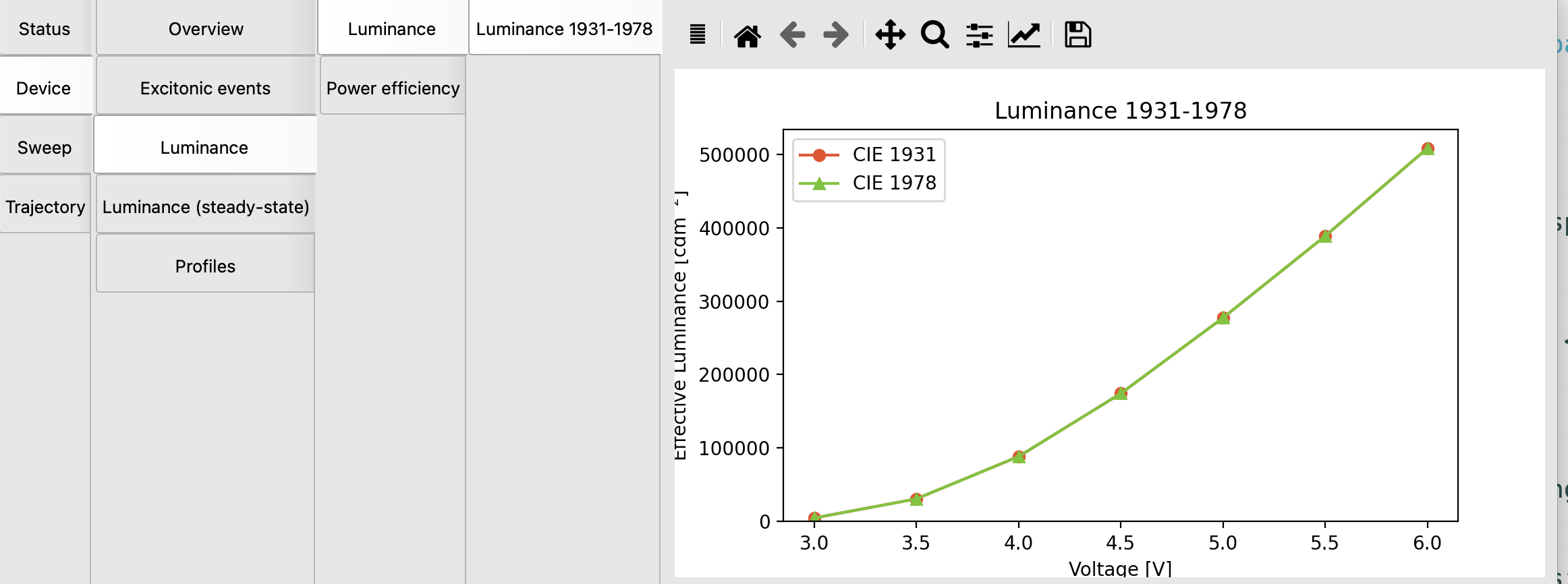
Fig. 45 The luminance increases with voltage
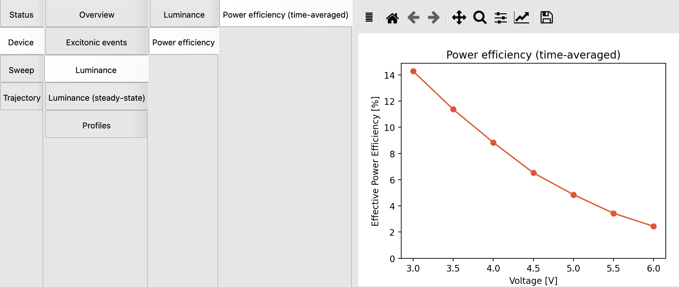
Fig. 46 The efficiency decreases rather strong with voltage