Device Equilibration
When an OLED circuit is connected, the voltage over the device gradually increases until steady-state conditions are reached. This voltage ramp can be included as part of the OLED simulation.
Circuit Closure
We will investigate circuit closure for the phosphorescent OLED constructed in the exciton tutorial.
Note
A pre-made project file is available for the circuit closure tutorial.
We open the exciton project using File → Open in BBinput. This will allow us to re-use the previously-constructed phosphorescent stack.
On the Parameters page, we will use the Load preset button to load the Single voltage point template. On the Main settings tab, we set the operating voltage to 5 V. The Excitonics modules should be enabled in the Modules tab.
In the Termination tab, we set the Convergence threshold to 0.05. This will automatically terminate the simulation once the system is within 5% of the steady-state current.
The Annealing and Equilibration tab allows configuration of the voltage ramp. We set the starting voltage to 0 V.
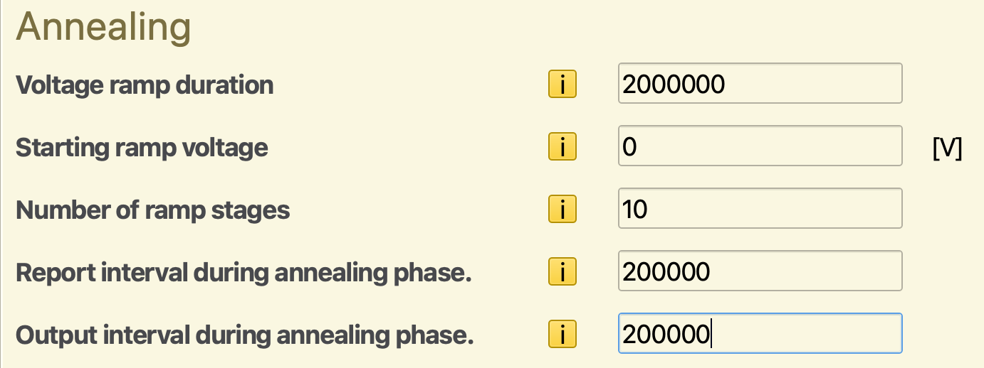
Fig. 116 Voltage ramp configuration in the parameter set
The ramp implementation increments the voltage over a fixed number of intervals, resulting in a stepped gradient. Here, we set the number of steps to 10.
The total duration of the voltage ramp is specified in terms of the number of Monte Carlo steps. We will use the first 2 output intervals. (These are set at 100,000 steps in the Output settings, giving us an annealing duration of 200,000 steps.)
Separate report and output intervals can be specified during the voltage ramp, allowing you to use different parameters compared to the rest of the simulation. In order to obtain output at the end of every ramp stage, we set both the report and output intervals equal to 1/10th of the ramp duration.
We can use File → Save and File → Run to start the simulation.
After the simulation has concluded, we can view the output with BBresults (SCM → BBresults). Transient current profiles can be viewed in the Sweep → Convergence → Overview section.
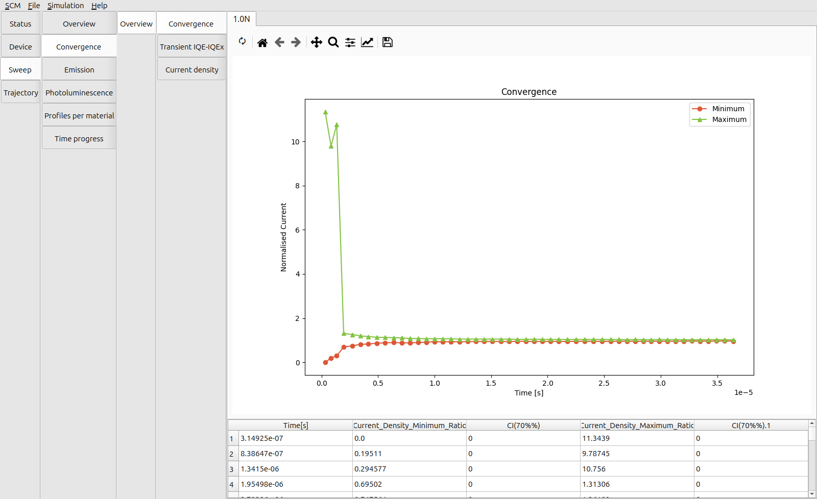
Fig. 117 Change in the transient current while simulating the circuit closure
When the voltage ramp is applied, charges are gradually accelerated towards the center of the emissive layer. This results in a faster approach towards the steady-state device current compared to a constant-bias simulation.
Circuit Disconnect
When the OLED circuit is disconnected, the external voltage drops near-instantly. This behavior can be investigated using the transient response feature.
During this process, we first want the device to be operating at steady-state conditions, i.e. having a stable internal field. A pre-equilibration stage may be specified in the simulation settings to allow the system to de-correlate from the initial state, approaching the device equilibrium. Simulation statistics will then only be generated for the samples obtained after pre-equilibration.
We load the annealing.bee project creating in the previous step. On the Parameters page, we will use the Load preset button to load a clean Single voltage point template. The starting voltage is kept at 5 V. Check that the Excitonics module has been enabled on the Modules tab.
The pre-equilibration is configured in the Annealing and Equilibration tab. We set a number of equilibration steps equal to 5 times the output interval. As with the voltage ramp, custom report and output intervals may be specified during the pre-equilibration stage. As we are interested in the dynamic behavior here, we will use the regular simulation intervals.
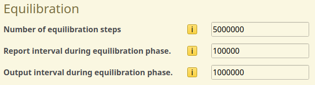
Fig. 118 Pre-equilibration stage in the parameter set
We will move to the Transient Parameters tab to configure the voltage switch. We create a new checkpoint at 10 microseconds, at which time the voltage will be set to 0 V.
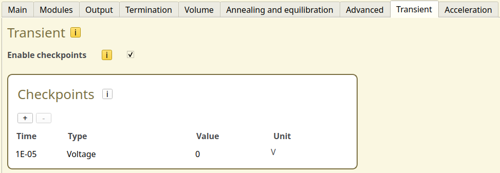
Fig. 119 We use a checkpoint to switch off the voltage from 5 V to 0 V after 10 microseconds
For this tutorial, we will only simulate a short window immediately after the device is disconnected. On the Termination tab, we set the Target simulation time to 100 microseconds.
We can use File → Save and File → Run to start the simulation. Once the simulation has started, we can monitor the output with BBresults (SCM → BBresults).
At the start of the simulation, the device current (Trajectory → Convergence → Overview → Trajectory Convergence) will behave as usual.
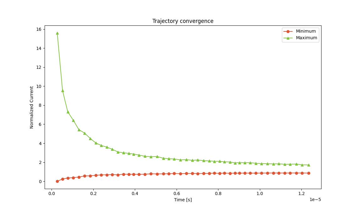
Fig. 120 Change in the transient current during the equilibration stage
As the equilibration phase proceeds, the device is gradually filled with carriers (Trajectory → Convergence → Overview → Current Density per Layer).
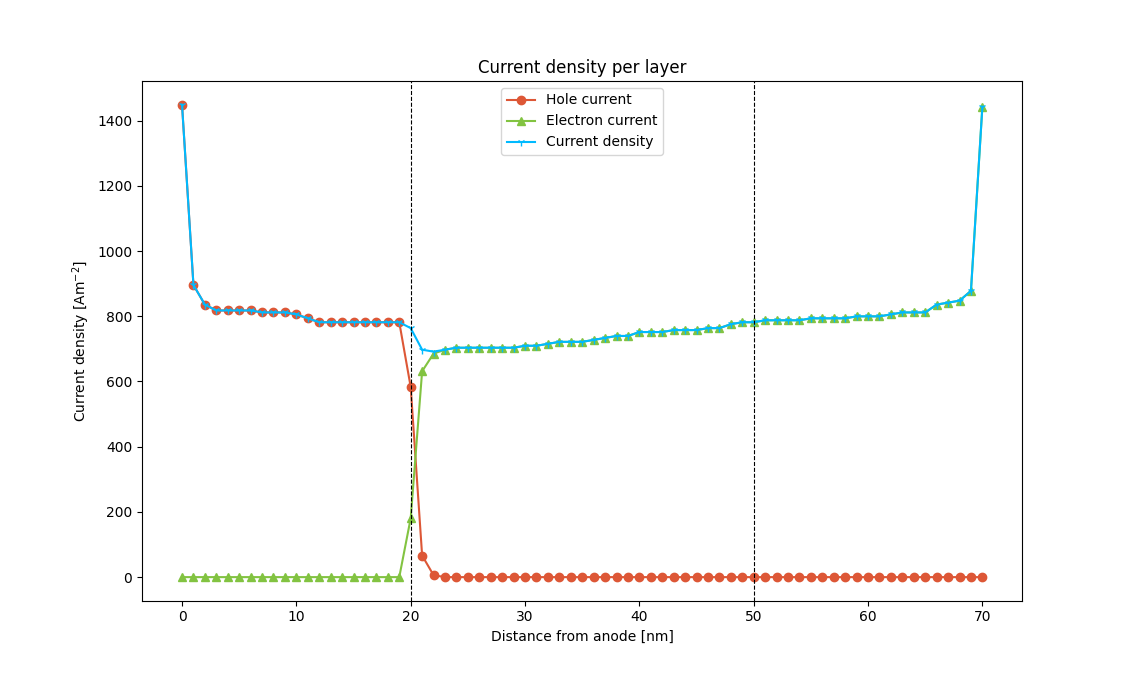
Fig. 121 Current densities at the end of the equilibration stage
Once the equilibration phase has ended, the simulation statistics will reset, such that the measured data will only cover the simulation window of interest. Meanwhile, the carrier distribution of the device is retained. The measurements therefore start from a pre-charged device.
When monitoring the graphs in BBresults, we can see when the reset in the statistics happens as the post-equilibration data replaces the figures.
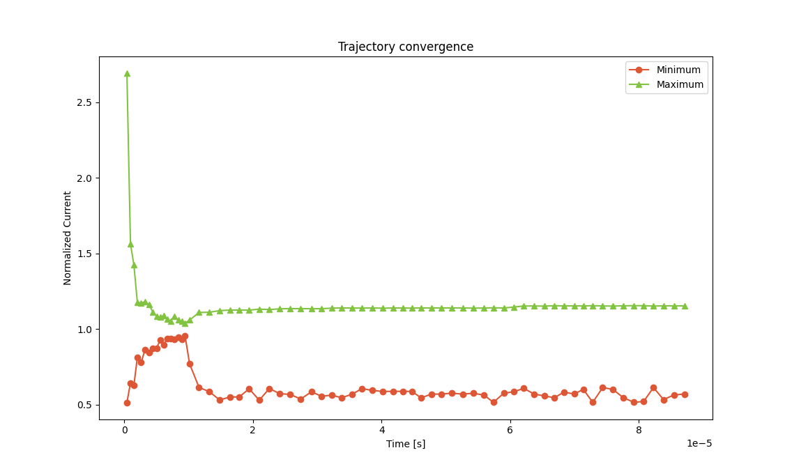
Fig. 122 Change in the transient current post-equilibration. (Samples generated during the equilibration phase are now omitted by BBresults)
The voltage drop was configured to occur after 10 microseconds. The offset is measured from the end of the equilibration phase. This is also why we did not see any changes in the device operation while the pre-equilibration was ongoing.
Once the circuit has been disconnected, a rapid drop in charge density is observed. Emission events (Sweep → Time Progress → Excitonic → Transient Radiative Exciton Decay Rate) continue to occur during a small window of time (around 5 microseconds). The residual charges in the device recombine near the emitters, causing the depletion of charges in the device.
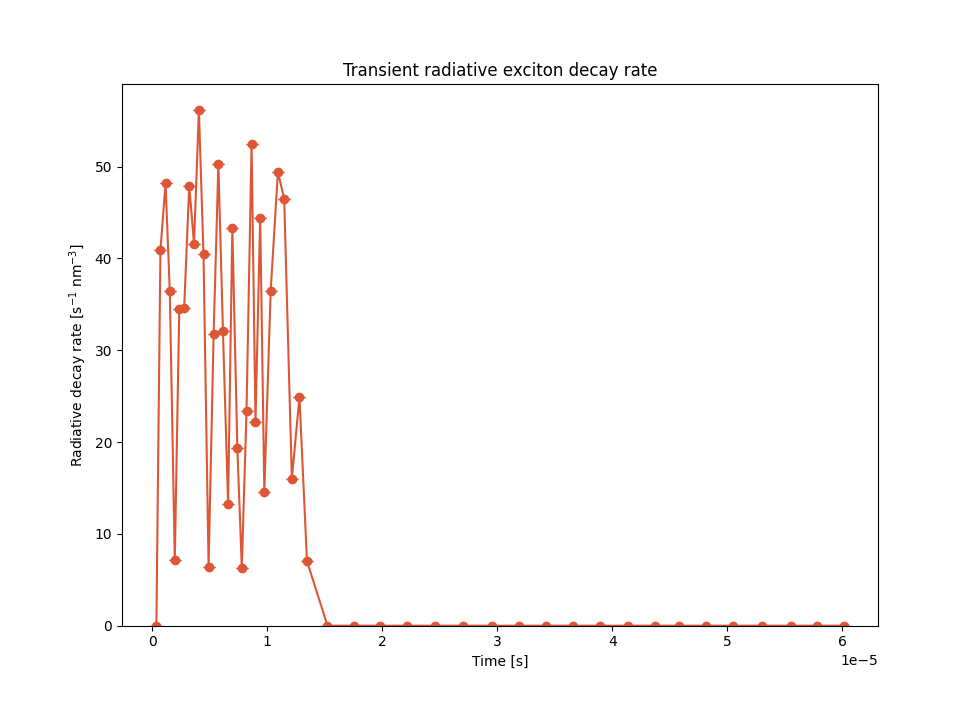
Fig. 123 Change in the emission rate post-equilibration
The exciton density (Sweep → Time Progress → Excitonic → Transient Triplet Density) rapidly approaches zero during this time.
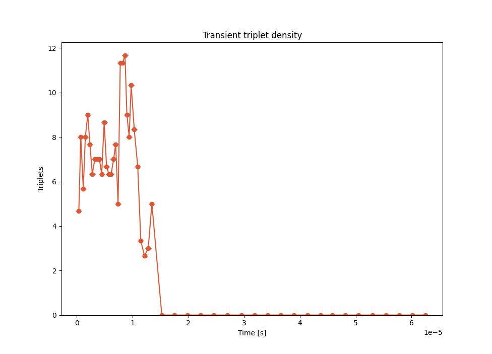
Fig. 124 Change in the triplet density post-equilibration
Residual charges (Sweep → Time Progress → Electronic → Transient Electron Density and Transient Hole Density) are seen to persist for a long time afterward, even after emission has stopped. These carriers are mostly located in the transport layers. With the electrons and holes located in different parts of the device, they are incapable of forming new excitons. In the absence of an external field, the mobility of the carriers is low, and recombination therefore takes a long time.
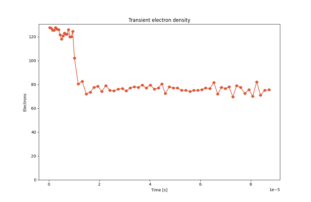
Fig. 125 Change in the electron density post-equilibration
For an OLED with a surface area of 2x2 mm\(^2\), a corresponding capacitance (Device → Overview → Performance → Capacitance) is calculated to be around 200 pF, which is typical for these types of 3-layer devices.
If the device where to be re-connected, the residual charges in the device would result in a shortened delay for emission to restart. However, care should be taken as a discharge into the external circuit can also occur.