Transient Switching
Bumblebee simulations can be used to investigate the response of organic electronic devices to external perturbations.
Here, we consider the effect of switching the device illumination on the current produced by an organic photovoltaic (OPV).
Note
A pre-made input file is available for this tutorial.
Load the OPV Device
A key benefit of Bumblebee projects is the ability to re-use materials, stacks or simulation settings. For this tutorial, we will be adding pulsed illumination to a photoluminescence simulation that was created in an earlier tutorial.
We open BBinput and use the File → Open option to load our project.
Note
The photoluminescence project file can be downloaded here.
Create a Bulk Heterojunction
The OPV layer materials are already available. For this tutorial, we will now be considering the photoresponse of a bulk heterojunction morphology for the OPV. (Compared to the bilayer device used previously.)
We navigate to the Compositions page and use the  button to create a new composition. By selecting the Morphology option, the composition editor will change to the Advanced Composition mode. While basic compositions are used to create ideal mixtures, advanced composition allow specification of gradients, inhomogeneous distributions or 3D systems such as polymer networks.
We will create an advanced composition using the PCBM and P3HT components. Select PCBM as the background material. Then use the button in the Morphology table to add a gradient. A linear gradient will be selected by default. The material can be changed to P3HT in the table.
When we select the linear gradient, an editor will appear below the table. Here, the material fractions at the layer boundaries can be set. We will have the gradient range from 0.8 at the start of the layer, to 0.2 near the end of the layer.
The morphology view includes a figure that previews the material distribution in the layer. We can enable the Normalize and Background options to view both components.
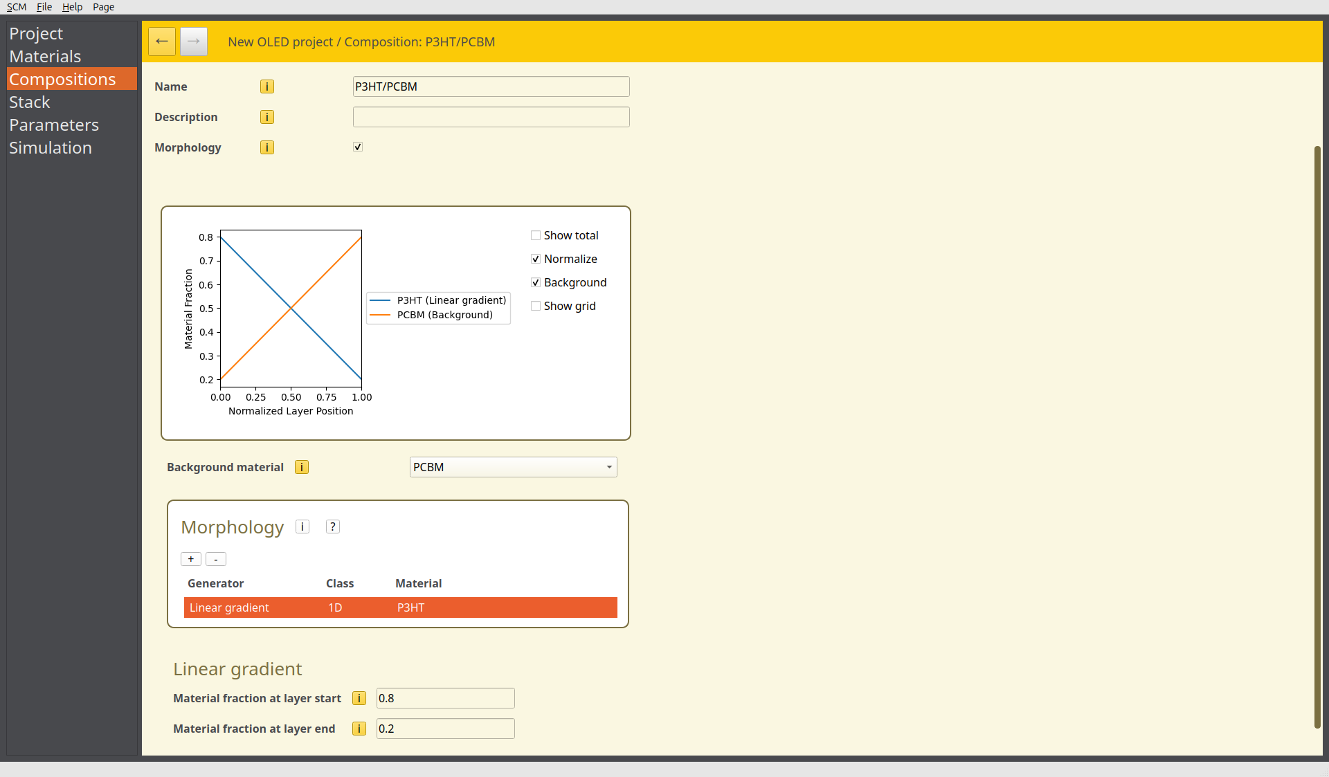
Fig. 95 Bulk heterojunction morphology preview in the advanced composition editor
By using the linear gradient, we have created a graded system corresponding to the interpenetrating phases of a bulk heterojunction. Save the new composition.
Update the Stack
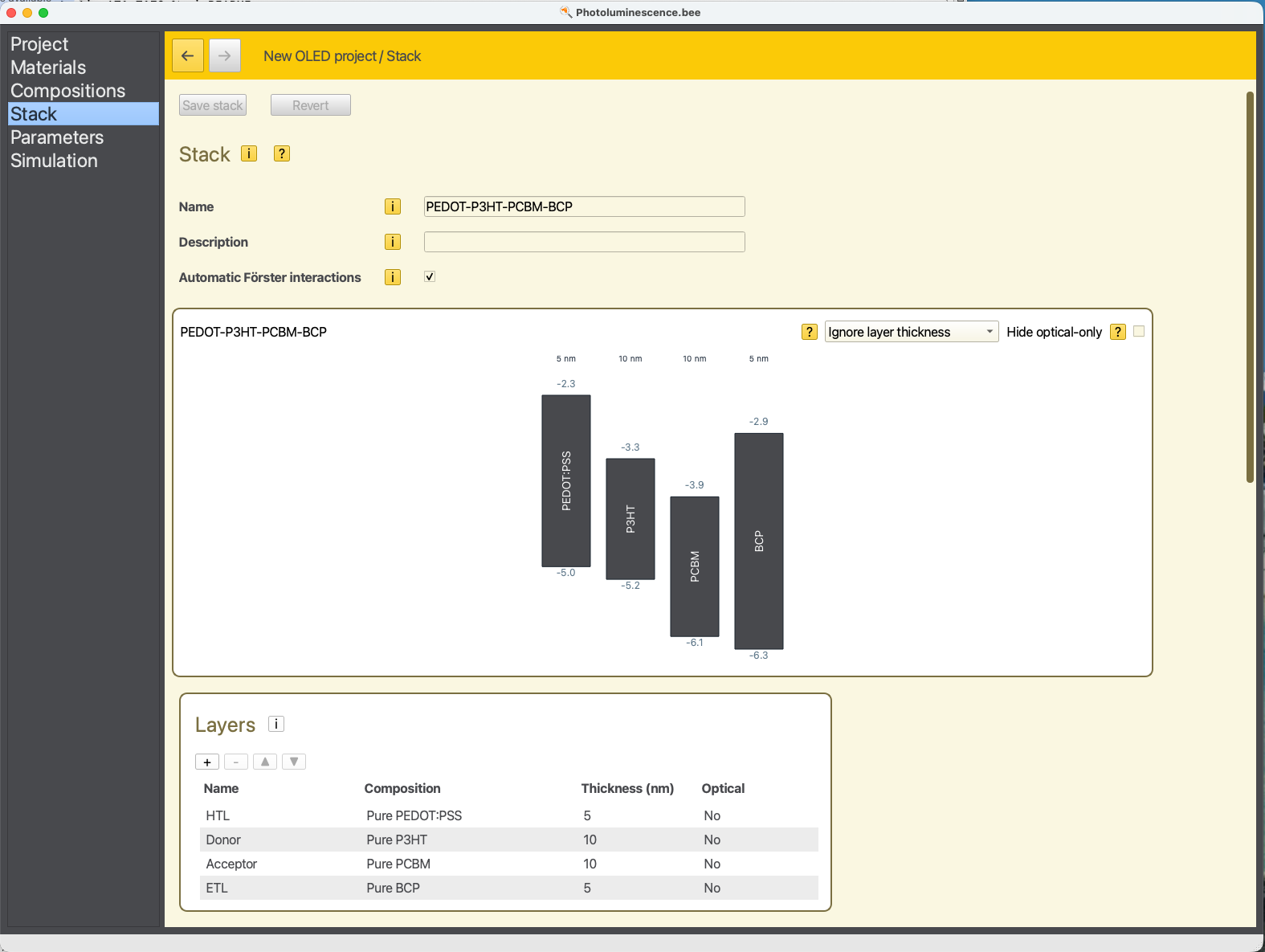
The OPV stack current contains separate donor and acceptor layers. We will now replace these with the heterojunction structure.
We need to remove the Acceptor layer from the Layers table shown below, but before we can do this, we first need to remove all references to that layer.
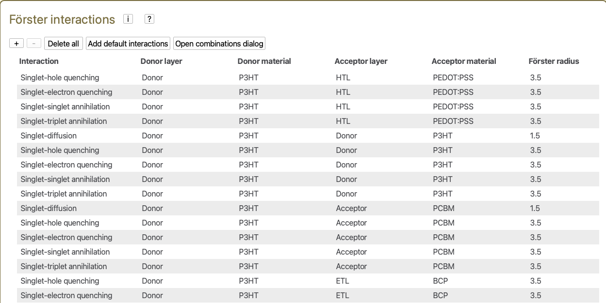
The first step is to uncheck the Automatic Förster Interactions checkbox at the top of the window depicted above. Then, we remove the existing absorption processes using the  button in the Absorption table.
Then, we click the Delete all option in the Försters interactions table.
Now, the Acceptor layer can be removed from the Layers table.
Next, we change the composition of the Donor layer to the PCBM/P3HT blend, and change the name of the layer to Junction.. The thickness of the layer is changed to 20 nm. The diagram will update to now show a mixed donor-acceptor system.
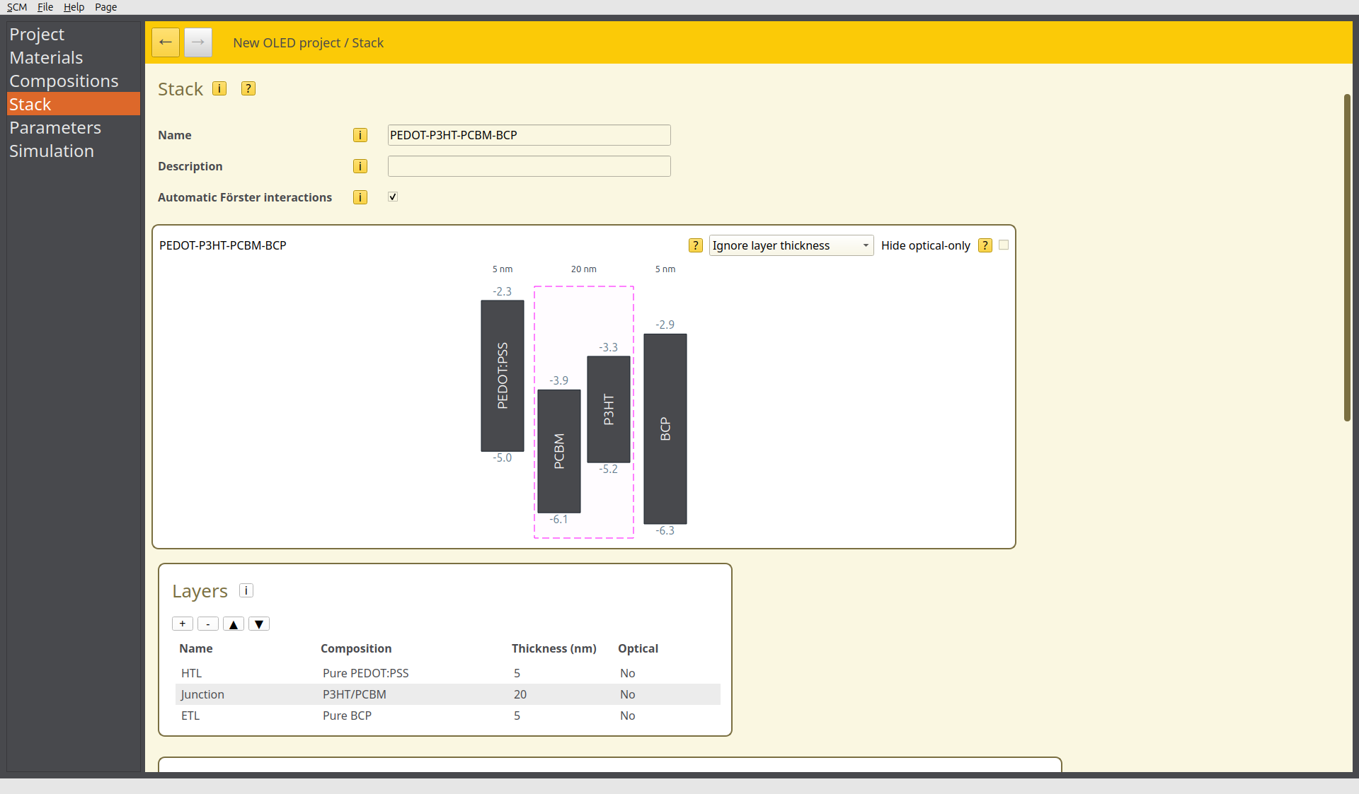
Fig. 96 Bulk heterojunction device in the stack editor
Recheck the Automatic Förster interactions option, to process the changes to the device structure when configuring the allowed Förster mechanisms.
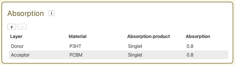
We add new absorption processes to both P3HT and PCBM materials in the heterojunction layer. (A new absorption process can be created using the button.) We use an absorption probability of 0.8 for both materials to account for optical loss processes. The singlet state is selected as the absorption product.
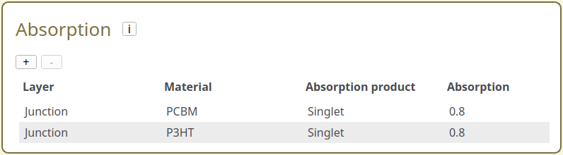
Fig. 97 Absorption configurations in the stack editor
Save the resulting stack.
Tip
For this tutorial, we focus on excitonic processes. In bulk heterojunction devices, geminate pair formation can also occur, wherein the positive and negative charge of the excited state become delocalized between donor and acceptor molecules. This affects the rate of charge separation in the junction. For donor-acceptor systems that feature strong delocalization character (e.g. fullerenes), the exciplex absorption product can be enabled to model the spatially-dependent field dissociation. Consideration of this effect becomes relevant when studying devices with space-charge limited photocurrent.
Transient Illumination
The Parameters have already been configured for photo-absorption simulations of an OPV device. We will now change to a pulsed illumination using the checkpoints feature.
Transient Switches
Perturbations to the device operation can be added in the Transient tab.
Checkpoints can be provided for various parameters, such as the voltage, current or fluence. Checkpoints occur at a designated time after the simulation has commenced. Multiple checkpoints of different types can also be combined to replicate complex interactions.
Device perturbations must first be activated by enabling checkpoints.
Individual perturbations can then be added to the simulation by selecting the button.
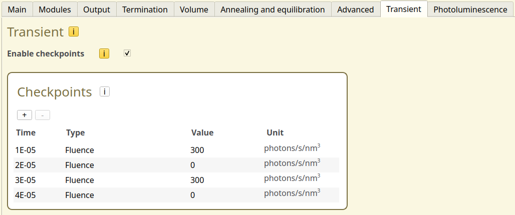
Fig. 98 Transient configuration for pulsed illumination
Light switching will be investigated by simulating 2 illumination pulses. We create a Fluence checkpoint at 10 microseconds, with a value of 300 photons/s/nm\(^3\). Additional checkpoints are added every 10 microsecond to alternate the fluence.
The starting fluence is set to 0 photons/s/nm\(^3\) in the Photoluminescence tab (tab labeled Fluence). A target simulation time of 10 milliseconds is specified in the Termination tab, at which point the simulation concludes. Save the parameter settings.
Tip
When performing continuous pulsing measurements, the pulses module can be used to apply a continuously varying signal, instead of manually entering checkpoints. This also allows specification of different pulse shapes, to more accurately replicate the signals encountered in measurement setups. Consult the manual for more information.
Starting the Simulation
Because we are simulating a fluence signal with a fixed illumination intensity, we will change the simulation to a voltage sweep. This will allow us to measure the field-dependence of the OPV current.
Navigate to the Simulation tab and set Sweep → Voltage. We run the sweep from 1 to 5 V in 5 steps.
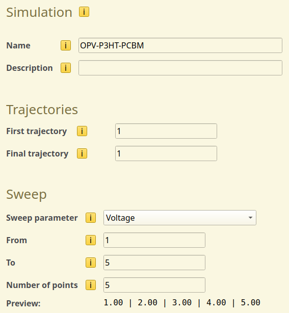
Fig. 99 Voltage sweep setup in the simulation settings
Use File → Save and File → Run to start the simulation.
Tip
If you wish to limit the computational time required for this tutorial, you can perform a single-point calculation (Sweep → None) instead. This will use the default voltage of 0.5 V defined in the parameter set.
Simulation Output
After the simulation has concluded, the transient response of the OPV current to the pulsed illumination can be viewed in the Sweep → Time Progress section of BBresults. The Electronic → Transient Electron Density tab shows the increase in charge carriers due to photo-absorption, which coincides with the pulse intervals.
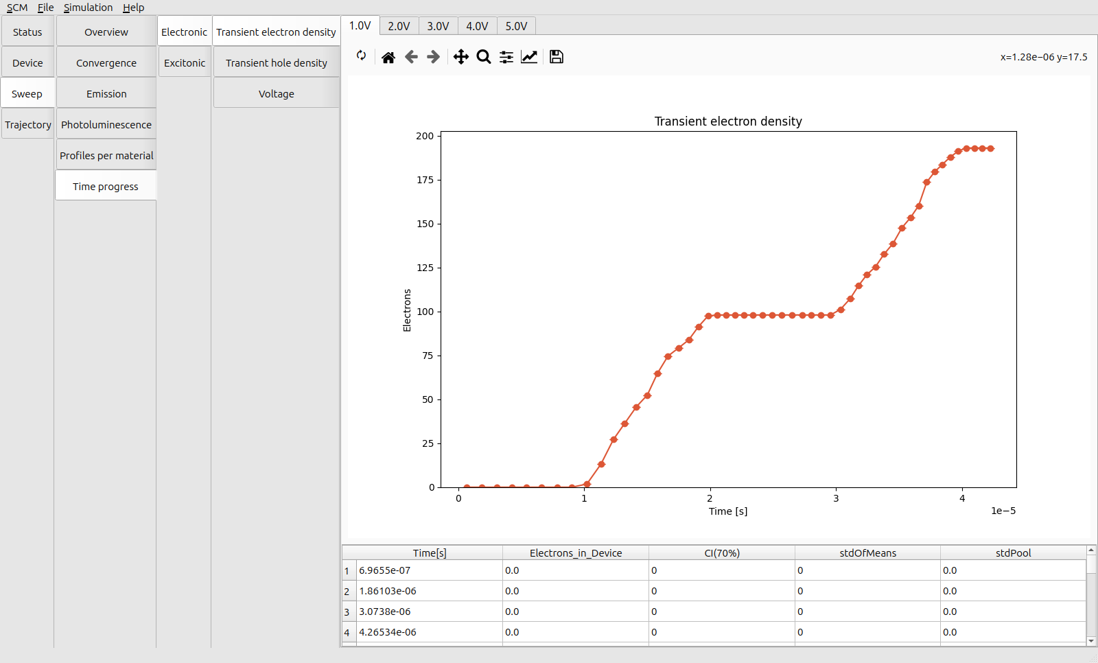
Fig. 100 Transient electron density during pulsed illumination at 1 V
The photo-generation of excitons is the dominant excitation mechanism at low voltages. The pulses are therefore similarly reflected in the transient IQE(x). The Convergence → Overview → Transient IQE-IQEx tab shows that some of the excitons are long-lived compared to the interval between the pulses, resulting in a smearing of the photo-response due to the presence of residual singlets.
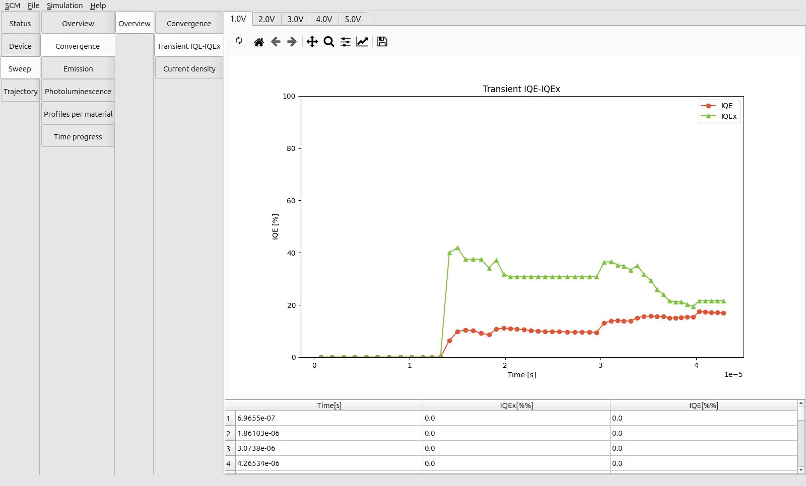
Fig. 101 Transient IQE during pulsed illumination at 1 V
This effect diminishes at higher voltages as a stronger field facilitates the dissociation of the excitons.
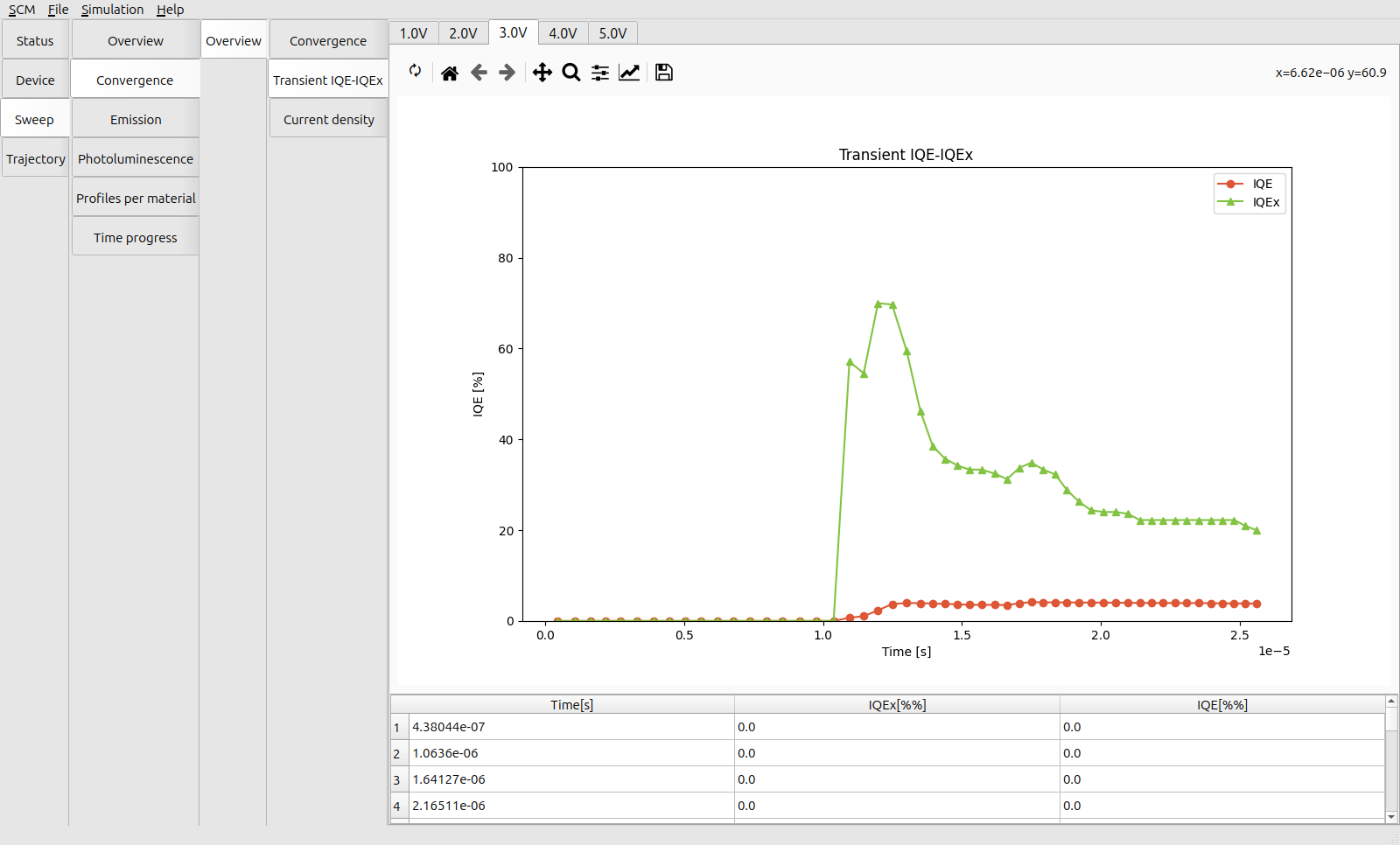
Fig. 102 Transient IQE during pulsed illumination at 3 V
These fluctuations in the charge carrier densities are also reflected in the Sweep → Convergence → Overview → Current Density. Although, for a single trajectory, the noise in the transient signal will probably be too high to distinguish any appreciable change in the current. Part of the reason for this is because the dark current has not yet stabilized at the start of the simulation. By adding a pre-equilibration stage, along with an increase in the number of trajectories, we can improve the signal clarity in our JV response measurements.