OFET Simulation
Organic field-effect transistors (OFET) utilize organic electronics as charge transport materials in molecular transistors.
OFET modeling in Bumblebee is performed by adding a source-drain field perpendicular to the primary gate electrodes. This allows the cross-current behavior to be modeled.
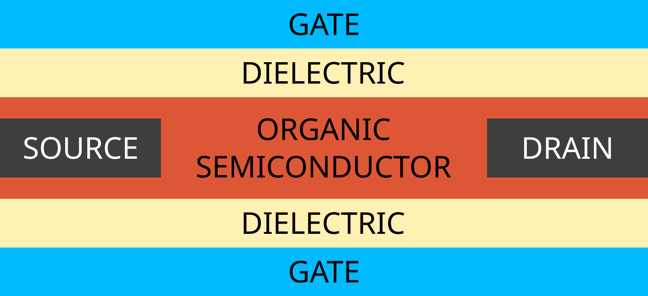
Fig. 103 Default probe-field OFET device geometry used by Bumblebee
The OFET device uses an organic conductor to channel carriers between the transistor source and drain. Dielectric layers are used to shield the gates.
Bumblebee uses 2 gate electrodes by default. In order to model single-gate OFETs, an insulator can be used to cut off access to one of the gates.
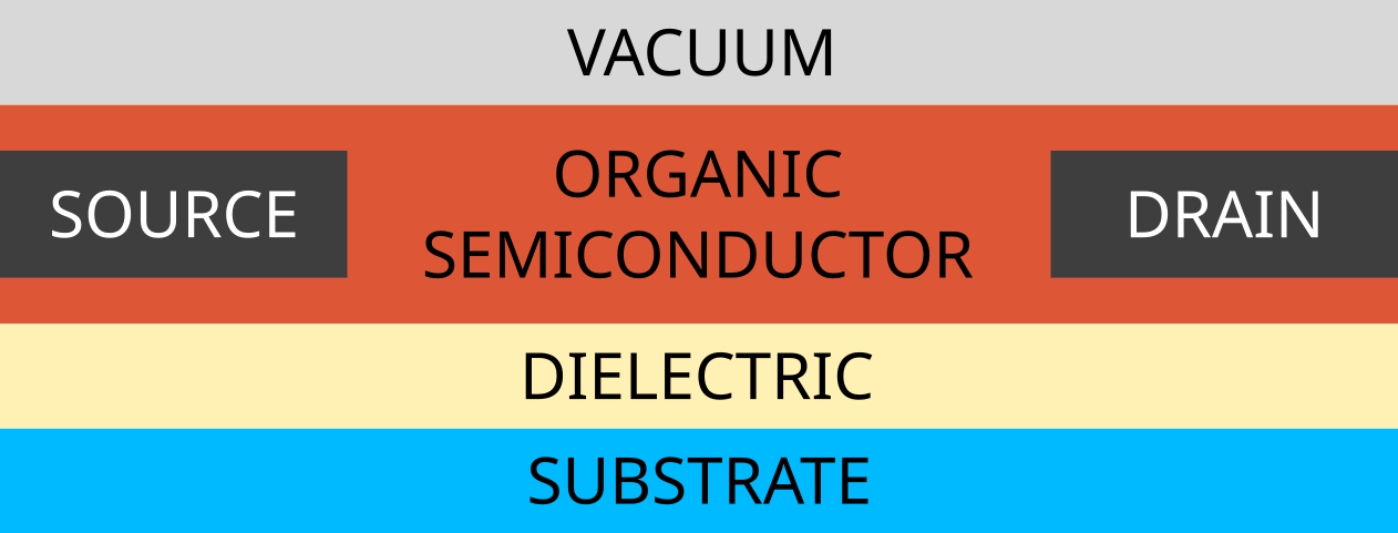
Fig. 104 Single-gate OFET device configuration
Create Materials
In this tutorial, we will discuss the modeling of an OFET memory device, using a charge trapping layer for polaron confinement.

Fig. 105 OFET memory device configuration (MOFET)
We will not focus on the role of excitons in this tutorial. For this reason, the OFET components will be treated as transport layers. (If desired, excitonic processes can be added to the OFET simulation to account for internal loss mechanisms.)
Conductive Layer
Pentacene is used in the conductive channel. To create a new material, go to the Materials page and use the  button. Click on the Transport Material template.
Add the name Pentacene and in the Electronic tab, set a HOMO level of -6.1 eV and a LUMO level of -3.9 eV. Change the electron mobility prefactor to 0.5 to study the effect of a slower diffusion rate of the electron species compared to the holes. Under Excitonic, we use a singlet binding energy of 1.2 eV and a triplet binding energy of 1.4 eV. Default Gaussian broadening is used for both polaron and exciton energy levels. Click on Save new material.
Dielectric Layer
SiO2 is used as a dielectric. For this, go to the Materials page and use the button to create a new material. Click on the Transport Material template.
Add the name SiO2. Under Electronic we set a HOMO level of -9 eV and a LUMO level of -1 eV. For Excitonic, we use a singlet binding energy of 2 eV and a triplet binding energy of 2.1 eV. Default Gaussian broadening is used for both polaron and exciton energy levels.
Both electron and hole mobility prefactors are set to 0.1 under Electronic to account for polaron blocking behavior of the dielectric.
In the Advanced tab, we can specify a source-drain injection prefactor. For the dielectric, this value is kept at 0 to block off the transistor contacts, which are meant to connect only to the conductive layer. Save this material by clicking on Save new material.
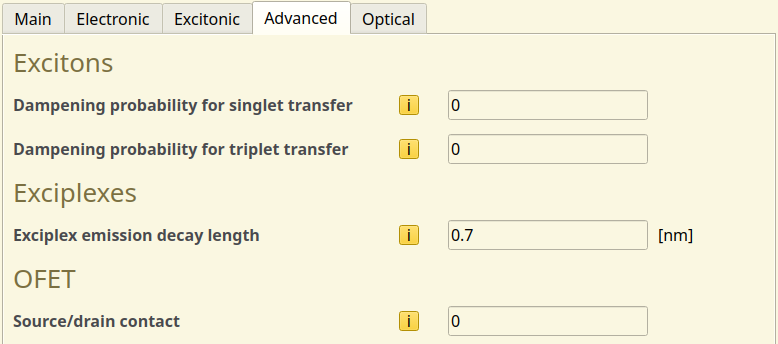
Fig. 106 Source-drain injection prefactor setting in the Advanced material configuration
Memory Layer
PVN is used as the charge storing material in the memory layer. We again use the Transport material template to create this material.
We set a HOMO level of -6.2 eV and a LUMO level of -1.2 eV. For the excitons, we use a singlet binding energy of 1.1 eV and a triplet binding energy of 1.5 eV. Default Gaussian broadening is used for both polaron and exciton energy levels.
The source-drain injection prefactor for the memory layer is set to 0, as only the conductive layer interacts with the transistor contacts.
Create a Stack
Under the Stack page, click on the button under Layers to create a new layer.
We will use the anode as the active gate. Therefore, we start by placing a 15 nm SiO2 layer. This is followed by a 10 nm PVN layer and a 35 nm Pentacene layer.
The Name, Composition and Thickness(nm) can be changed by double-clicking on it.
On the top right of the image, change the option to Full layer thickness. The input should be the same as shown in the figure below.
Click on Save stack to save the input.
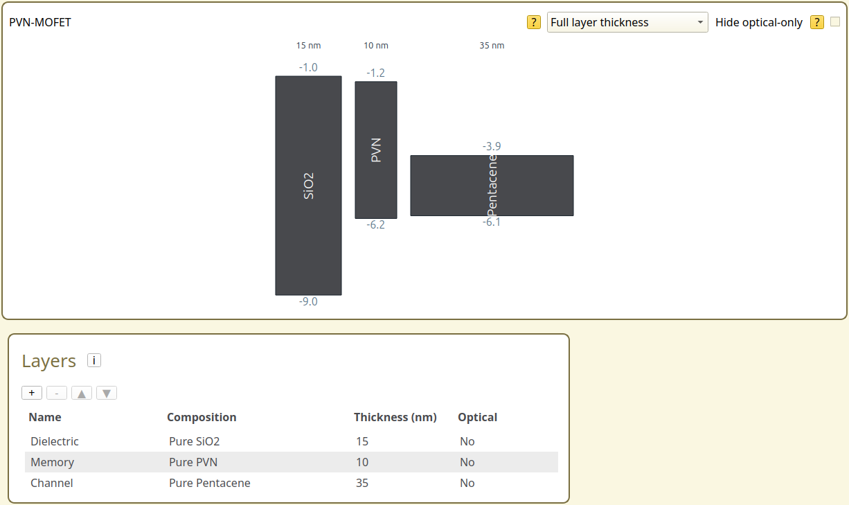
Fig. 107 PVN-MOFET stack setup in BBinput
Create a Parameter Set
Navigate to the Parameters page in BBinput. Select Load preset and choose the OFET template. This will automatically enable the Transistor module in the parameter set, which adds the source-drain contacts to the device. Polaron injection at the gates is also disabled. This prevents polaron hopping into the vacuum.
Note
If you want to model the OFET in a cross-current setup, with active gates, electrode injection can be re-enabled by adjusting the injection and collection prefactors in the Advanced tab.
Note
The exciton module is not enabled by default in the OFET template. If you want to model excitonic processes inside the OFET, remember to manually enable this module.
Note that the source-drain contacts are not shown in the (one-dimensional) energy level diagram. The location of the source-drain channel is instead controlled by the source-drain contacts set in the material parameters.
We now proceed to configure the gate contacts. On the Main tab, the device voltage is set to 10 V. The anode contact is taken as the transistor gate. We assume a Au contact and set the Fermi level to -5.1 eV. The cathode will represent the interface with the air. We set the Fermi level to 0 eV to avoid interactions with the device.
The OFET tab allows configuration of the transistor voltage. The drain-source field is initially set to 3 V. Technical parameters are provided for controlling the gate field.
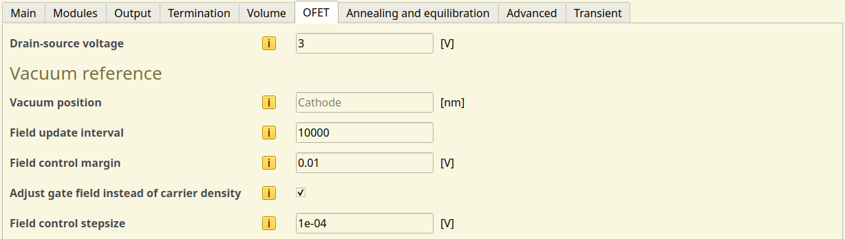
Fig. 108 Transistor configuration in the parameter set
The single-gate transistor has zero electric field at the vacuum interface. This condition is maintained as charge carriers populate the device, resulting in a change in the electric field inside the stack.
An update is performed at a given field check interval to correct the gate field for the changing polaron distribution. By default, this is implemented as an external field correction. The field is adjusted incrementally using the field control step size. Alternatively, polaron exchange with the gate can be enabled to adjust the carrier distribution.
To avoid oscillations in the electric field, a field control margin is defined. Field updates are only performed when the gate field error exceeds this value.
The adjustment to the gate field is performed to maintain the vacuum level. The position of the vacuum is located at the cathode by default.
Save the parameters.
Starting the Simulation
Sweeps of the gate voltage can be used to obtain OFET transfer curves. For this tutorial, we perform a voltage sweep from -10 to 10 V using 11 steps. Due to the limited disorder in our MOFET materials, we will only set a single trajectory. Use File → Save and File → Run to start the simulation.
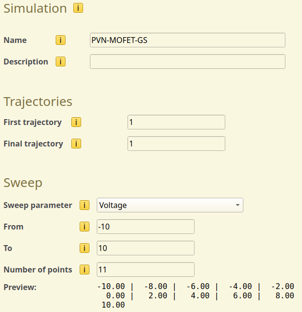
Fig. 109 Gate-voltage sweep configuration in the simulation settings
Tip
Parameter sweeps can also be performed for the drain-source field strength to investigate the effect of cross-field interactions on the device current.
See also
To simulate memory programming/erasure cycles, transient switches can be used to adjust the device polarity during the simulation. Consult the transient response tutorial for more details.
Simulation Output
To check the results of the simulation, open BBresults by going to SCM → BBresults and load the .bee file.
Polaron mobility, channel conductivity and transfer curves are available in the Device → OFET section of BBresults. The output is split into 2 tabs: Simulated and Interpolated. The Simulated tab contains the simulation output of the voltage sweep. The Interpolated tab post-processes the results to construct more detailed transfer curves. This typically produces more accurate voltage-dependencies (particularly near 0.0 V). We will therefore focus on the Interpolated output here.
The Drain-source polaron mobility curves report the effective channel conductivity and effective mobility of the carriers inside the MOFET. The values that we see here are typical for organic electronic materials.
The conductivity of electrons is approximately twice as high as for the holes. This is also reflected in the measured currents, which can be attributed primarily to a lower saturation density for the electrons. In turn, similar values are obtained for the effective mobilities as these are mostly determined by the transport through the pentacene layer.
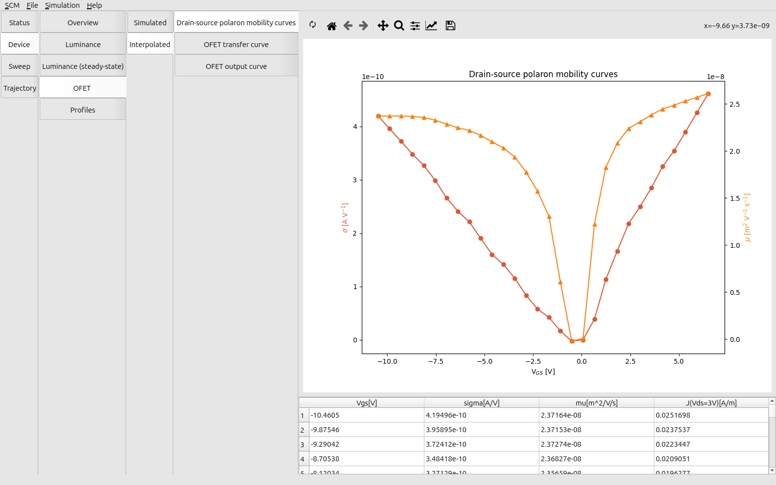
Fig. 110 Mobility and conductivity measurements for the PVN-MOFET
We can visualize the accumulation of charges from the Device → Profiles → Electron Density per Voltage and Hole Density per Voltage tabs. At positive voltages, electrons are injected into the device. Hole injection occurs at negative voltages. Our source-drain contacts are connected to the pentacene layer. Injected electrons do not go into the PVN memory layer due to the high energy barrier between LUMO states. This confines the electrons to the channel, resulting in a shorter effective path length and a higher effective mobility.
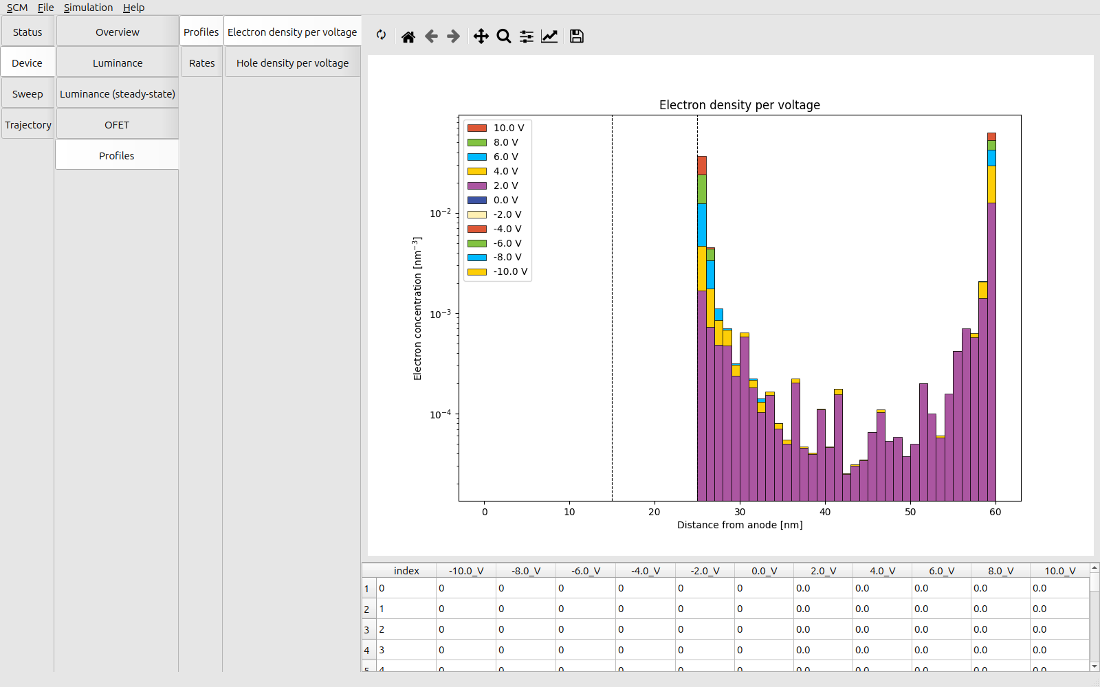
Fig. 111 Voltage-dependent electron density in the PVN-MOFET
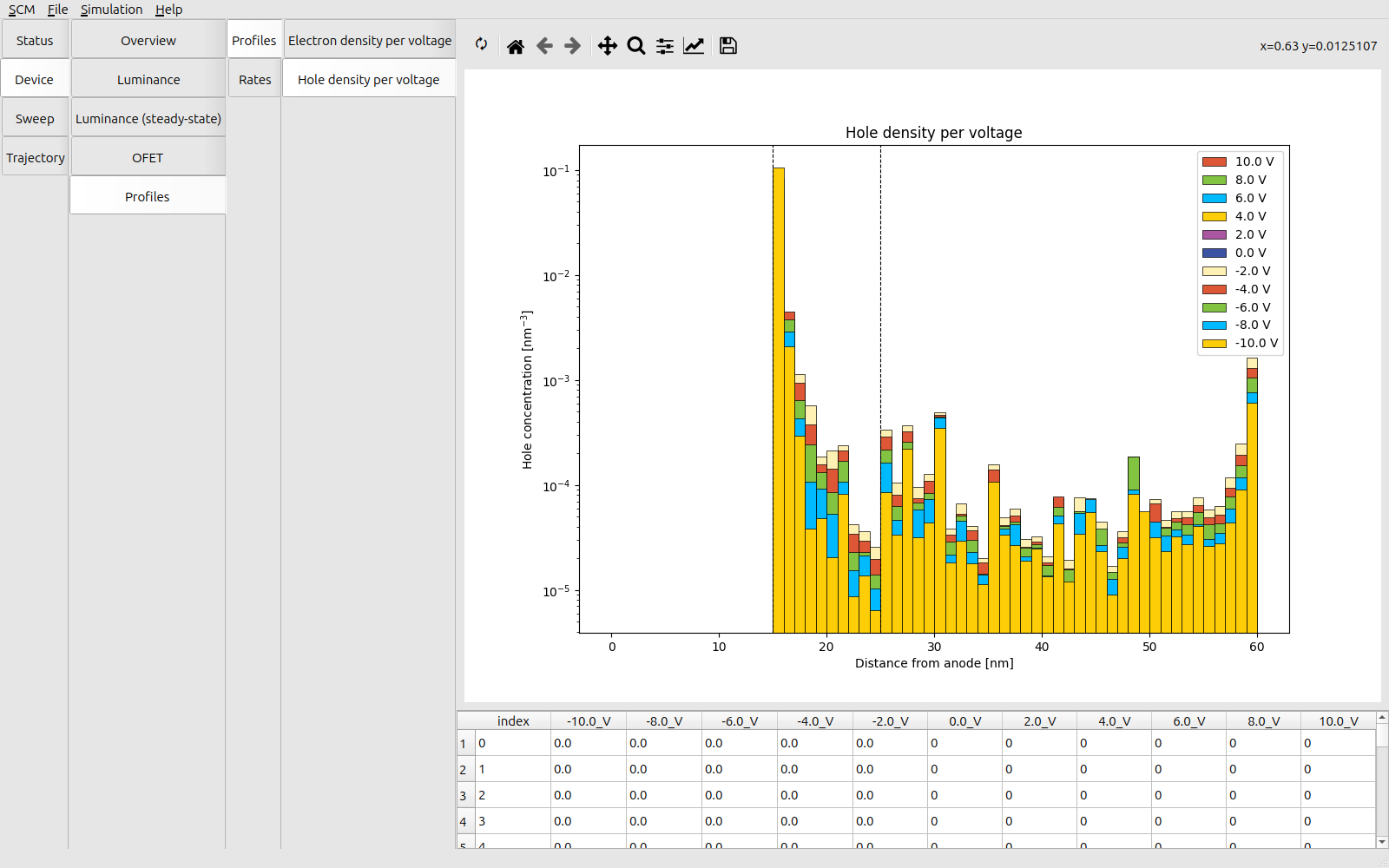
Fig. 112 Voltage-dependent hole density in the PVN-MOFET
We can view the electrostatic potential inside the OFET stack (Sweep → Overview → Profiles → Potential). The gate field inside the semiconducting channel has been screened. Polarization is therefore confined to the dielectric layer.
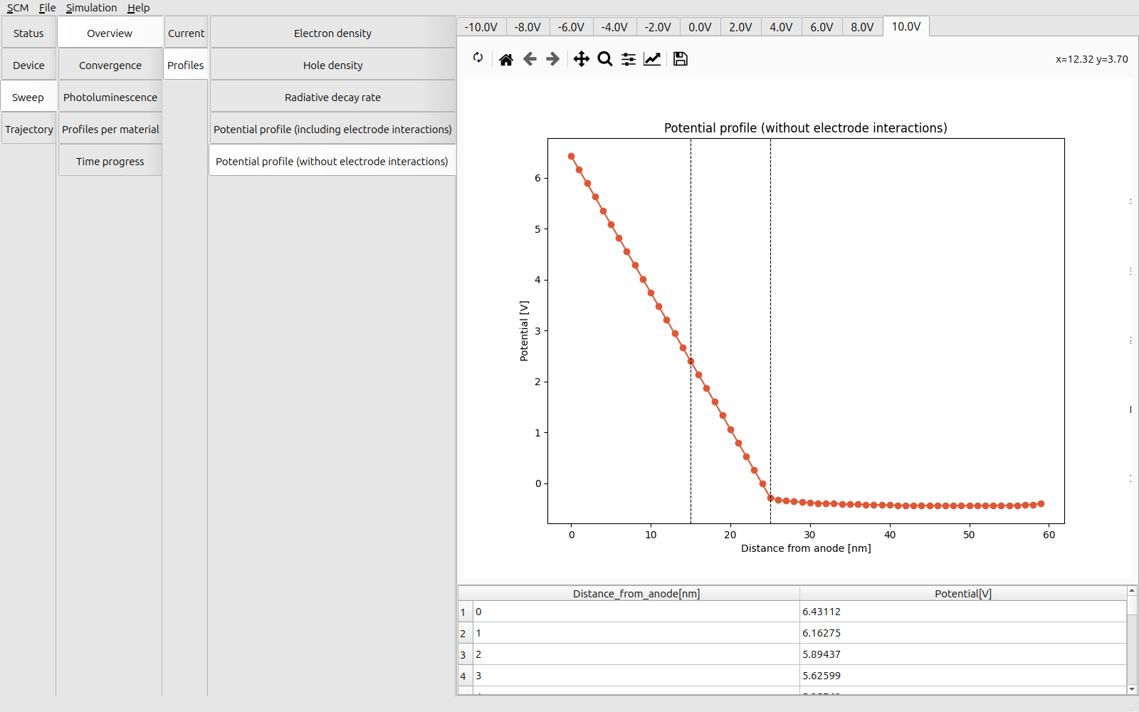
Fig. 113 Electrostatic potential profile at forward gate bias
The transfer curves of the OFET are available in the Device → OFET → Transfer Curve section. These curves show the saturation of the drain-source current in relation to the applied gate voltage. The drain-source current is proportional to the effective conductivity within the simulated regime. This indicates a limited co-axial transport through the PVN memory layer. Charging of the memory therefore occurs primarily through exchange with the conductive transistor channel.
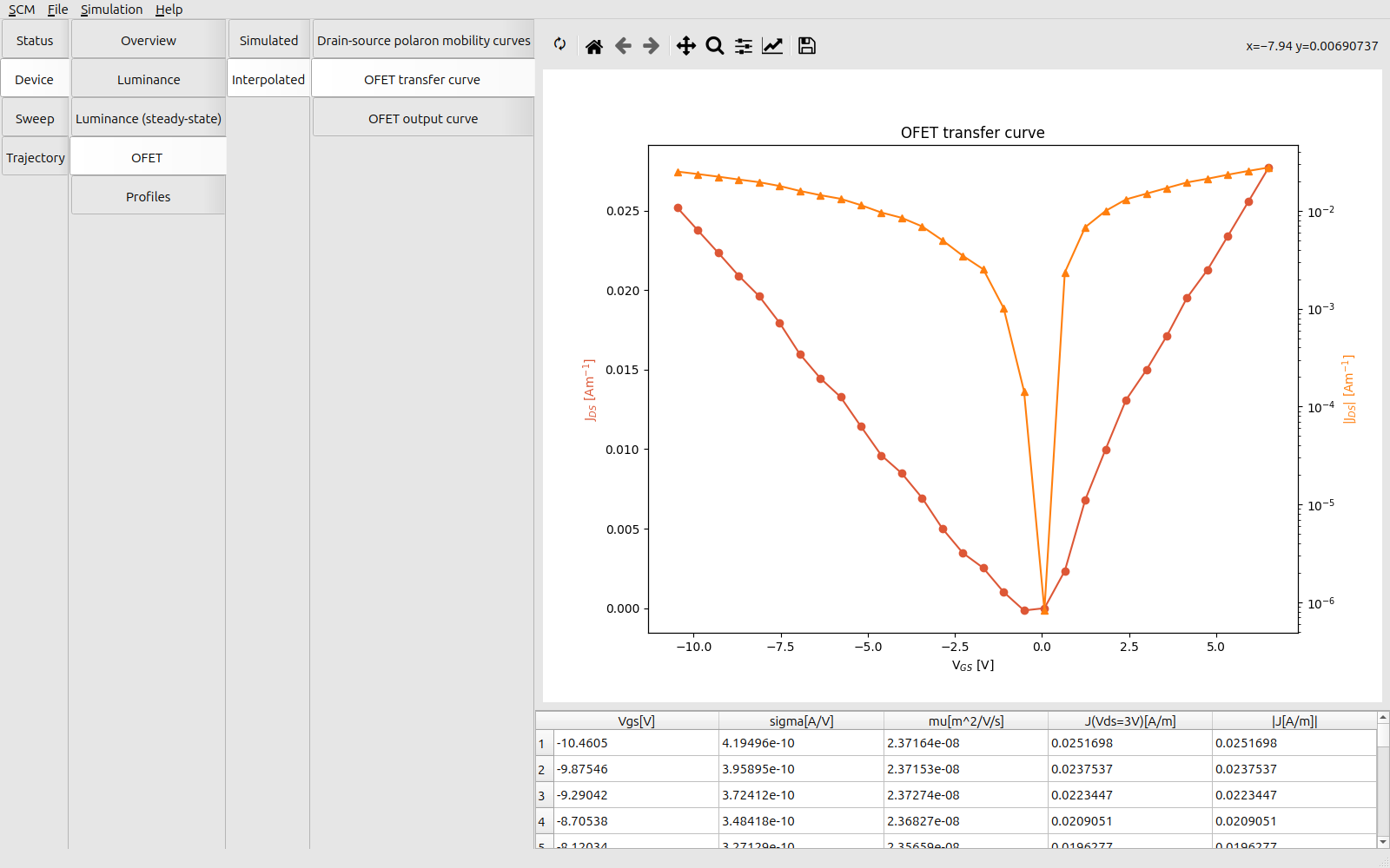
Fig. 114 Transfer curves for the PVN-MOFET
The output curves of the OFET are available in the Device → OFET → Output Curve section. These curves provide the JV characteristics of the drain-source channel at various gate voltages. An increased gate voltage enhances the polarization of the dielectric, creating the field effect that enhances the transistor conductivity. We can see that the PVN-MOFET is operating in the linear regime, with sub-saturated currents.
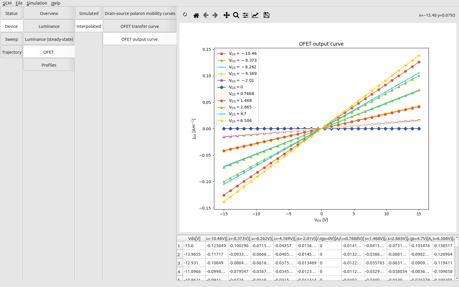
Fig. 115 Output curves for the PVN-MOFET
At higher drain-source voltages, higher charge densities in the device may cause the output curves to level off as the conductive channel is filled. Excitonic events may also introduce additional loss processes at higher carrier concentrations, resulting in non-ideal efficiencies.