Closing the band gap of a 2D semiconductor with an electric field
This tutorial focuses on a monolayer of Molybdenum disulphide MoS2, because this material is of interest for transistors, in particular the switching to and from a conducting state. It is based on a CECAM workshop exercise.
Create the MoS2 monolayer
You can use the MoS2 monolayer from our database, follow step 1 of the MoS2 response tutorial.
Analyze the DOS and band structure
Symmetric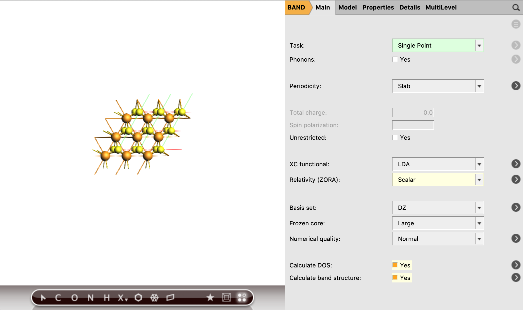
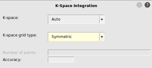
Note
For some materials, like the MoS2 monolayer in this tutorial, the high symmetry k-points are important. For those materials, it is important to sample the k-space symmetrically.
After the calculation is finished, the band structure can be visualized.
The bands are colored according to the main contribution, also known as ‘fat band analysis’. The band structure will look as follows:
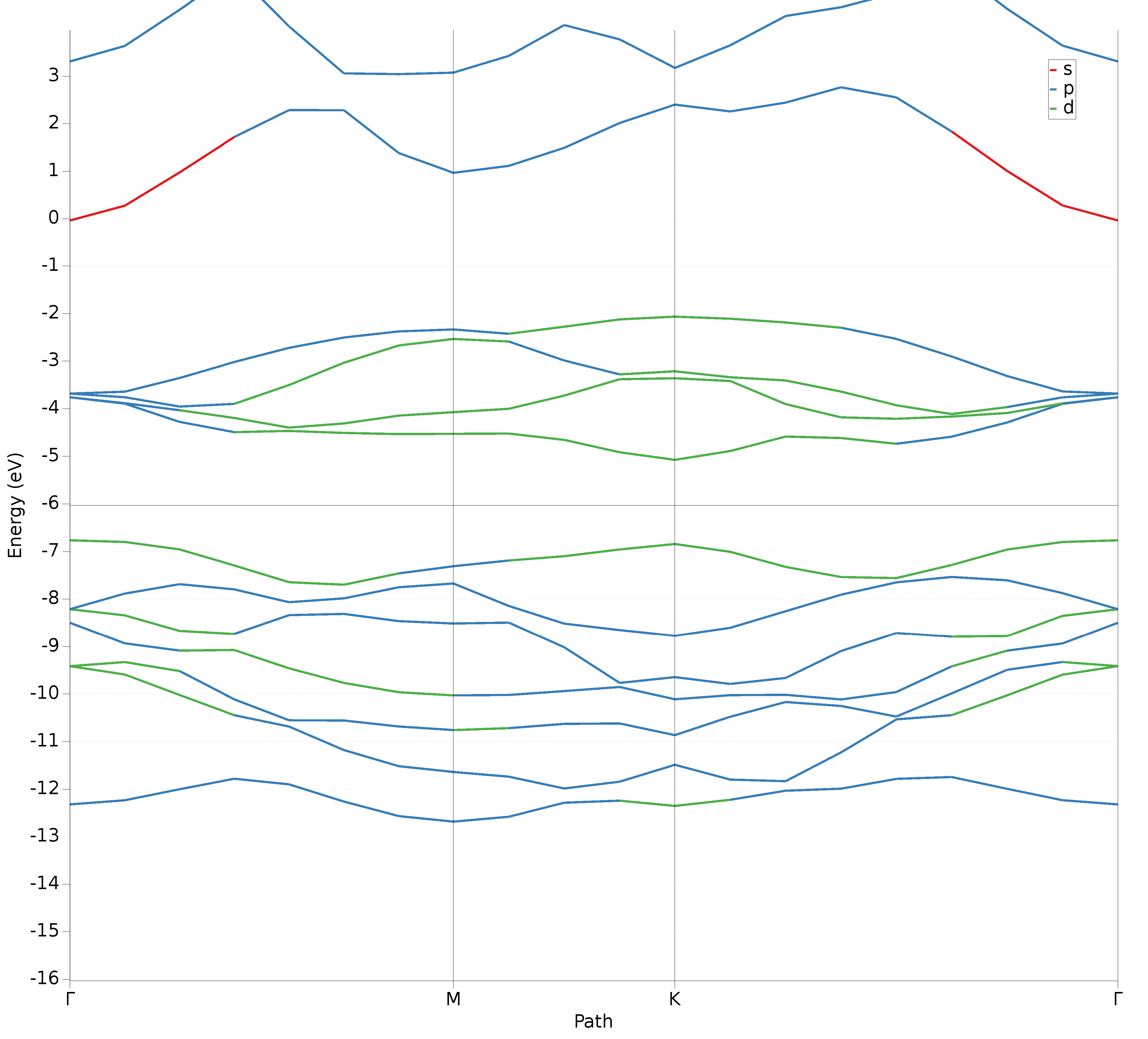
To receive band structure curves that are more smooth, the delta-K parameter of the interpolation can be adjusted.
0.03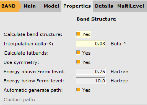
The bands should look much more smooth now. If you zoom in and hover over the bands you should see an indirect band gap from the gamma point to the K point, which is on the edge of the Brillouin zone. (See the indirect band gap at the horizontal black line.)
Electron-hole transport
For semiconductors the shape of the bands near the Fermi level tells you something about how easy the electrons (in the bottom of the conduction band) or holes (in top of the valence band) can move. The inverse of the curvature is called the effective mass of the electron or hole. A small curvature means a large effective mass of the electron or hole, and a large curvature means a large effective mass. To calculate this effective mass:
Tip
See also the BAND tutorial Band Structure and Effective Mass Tensors of Phosphorene
Fix the band gap
The band gap (as read from the band structure plot) is about 1.7 eV, whereas experimentally it is 1.9 eV (see e.g. Heinz et al. [1] ) We have used the LDA functional, which is known to underestimate the gap. You could try to improve the band gap by using a model potential. For systems that are not crystals, the most convenient choice is the GLLB-SC functional. (XC functional: Model → GLLB-SC) Now the Quasiparticle gap should be a bit higher, since the GLLB-SC includes explicitly the so-called derivative discontinuity. The SCF convergence can be more difficult with GLLB-SC. We leave it as an exercise to find good settings for GLLB-SC. Consider increasing the basis set, modifying the k-point grid or changing the SCF Method in any of the Details panels.
Note
The band gap in the log file can be different from the one obtained from the band structure. This is because the k-points are different in the initial calculation and the subsequent band structure calculation.
Applying an electric field
An electric field will reduce the gap significantly. You will need quite strong fields to make the material conducting.
3.0 V/Å.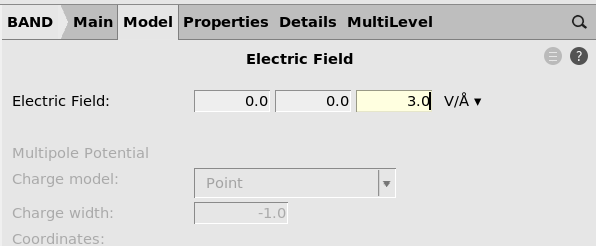
You will find the band character can change a bit at higher fields and you could determine through multiple calculations at what field strength the material will become conducting.
Analyzing the charge
The charge can be analyzed after you applied an electric field.
At a field of 3 Volt/Angstrom and some tweaking (You can change these features by opening the details by clicking the arrow in front of Plane: Colored)
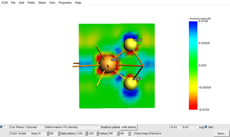
Here you can see that the charges on the two different S atoms are different because of the electric field.
Improving the accuracy
Many aspects influence the results of a calculation. Some are technical, such as the choice of basis set, k-points and integration accuracy; other are theoretical, such as the choice of functional. You can also consider computationally more expensive spin-orbit coupling instead of scalar relativistic. The relativistic effect is small for light atoms and grows with the charge of the nucleus.
The choice of XC functional is not so straightforward. However, to use a GGA is generally better than using the plain LDA. Among the GGAs the PBE functional is a reasonable choice or more modern metaGGAs such as MN15L and SCAN. Finally, the DZ basis set is usually too small, and one should preferably use a TZP one. For the gap (especially when p-electrons are involved) also the spin-orbit might be needed.