TD-CDFT Response properties for a 2D periodic system (NewResponse)
BAND can calculate response properties such as the frequency-dependent dielectric function within the theoretical framework of time-dependent current density function theory (TD-CDFT).
This introductory tutorial will show you how to:
Set up and run a BAND single point calculation (using AMSjobs and AMSinput) for an MoS2 monolayer
Set up and run a BAND TD-CDFT, linear response calculation (using AMSjobs and AMSinput) with the
NewResponsemethod for an MoS2 monolayerVisualize the dielectric function using AMSspectra
If you are not at all familiar with our Graphical User Interface (GUI), check out the Introductory tutorial first.
Step 1: Create the system
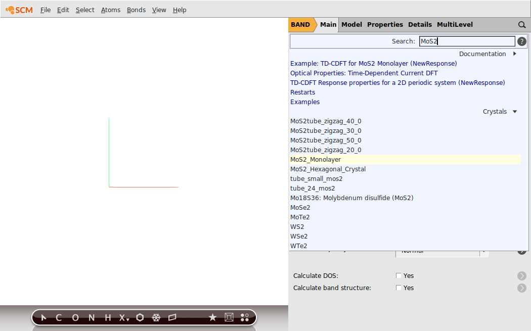
We now want to create a MoS2 monolayer. Let us import the geometry from our database of structures
 →
→ 
 .
.
If you succeed, your GUI should resemble the following picture:
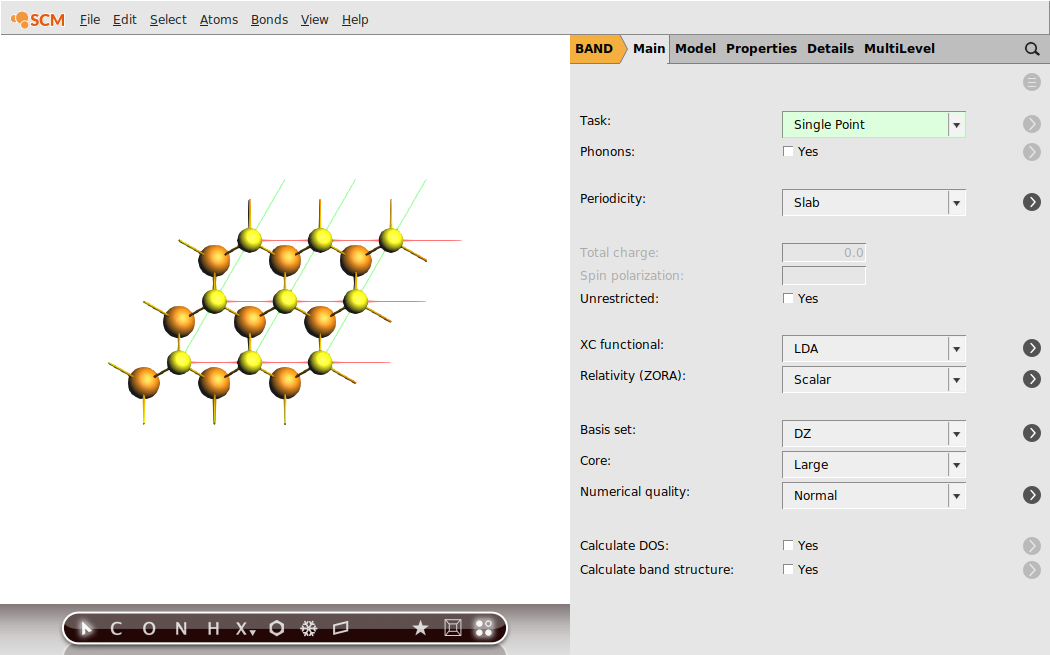
Step 2: Run a Singlepoint Calculations (LDA)
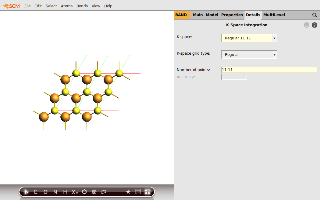
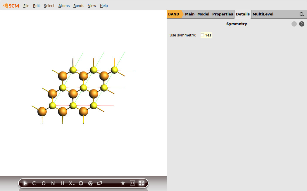
To get an idea regarding the performance of the LDA XC functional for the MoS2 monolayer, we first run a single-point calculation with the aim of analyzing the resulting band structure. We will already chose the calculation settings to be the same as for the following linear-response calculation with TD-CDFT: e.g. the basis set, the numerical quality, use of symmetry and the sampling of k-space.
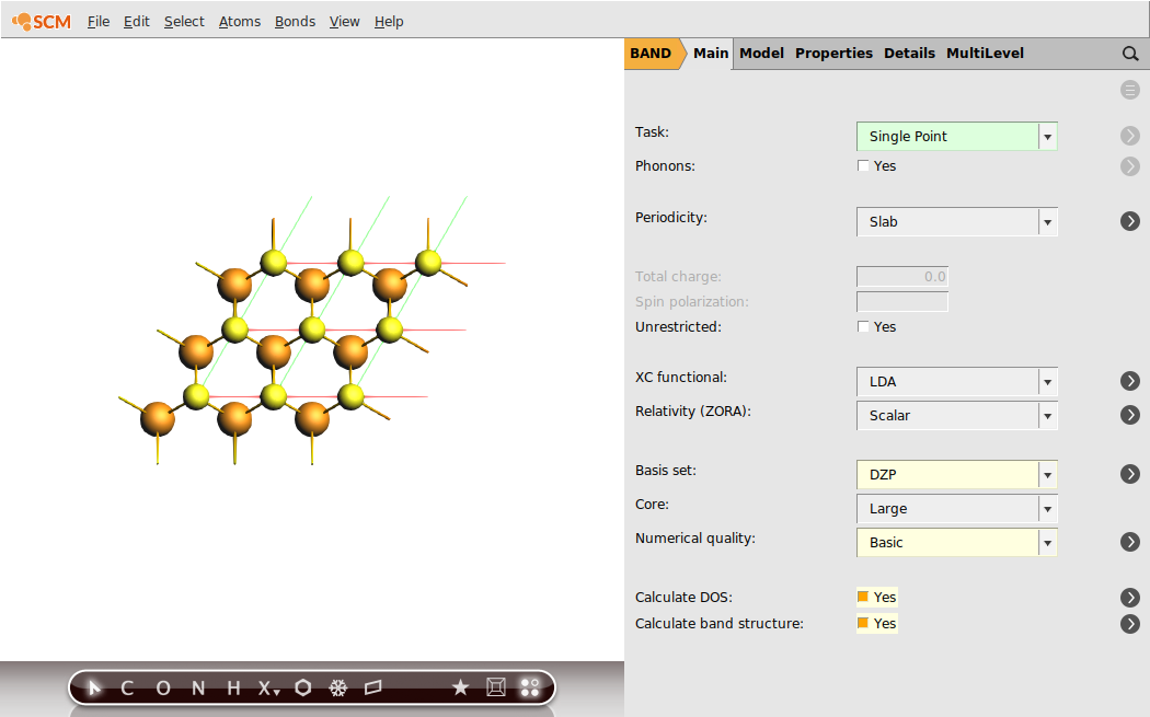
Now, everything is prepared for the single-point calculation.
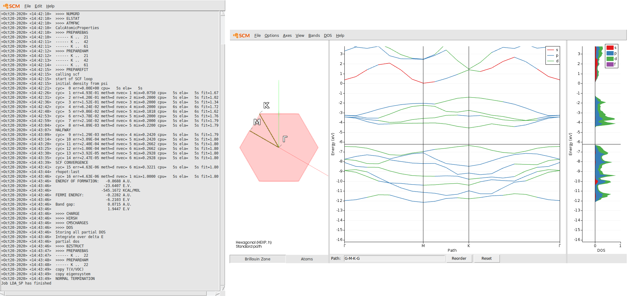
With the help of the bandstructure we can validate that basic electronic properties are reproduced by this k-space sampling using only LDA as XC functional. Unlike the multilayered MoS2, which has an indirect band gap, the MoS2 monolayer has a direct band-gap. (see also Ref)
Step 3: Run an NewResponse Calculation (ALDA)
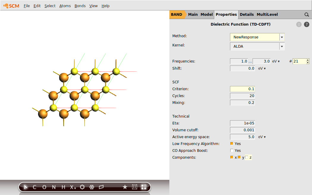
We can now start the calculation of the frequency-dependent, dielectric function using linear response TD-CDFT. As a reasonable frequency range we shall sample from 1.0 eV to 3.0 eV with a step size of 0.1 eV.
Tip
The absolute values of the dielectric function depends on the assumed two-dimensional volume for the surface. Since this definition is arbitrary, you can change the value for the Volume cutoff, so that the static dielectric function is reproduced.
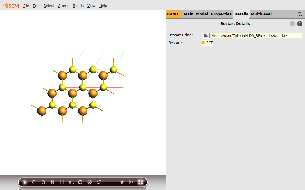
Since we have already calculated the SCF results in the previous run, we can restart the SCF from the band.rkf file (this will save some time during the SCF procedure)
Tip
This allows us to split the frequency range into smaller parts without too much of an overhead due to the SCF convergence for the ground state properties. One could even think about restarting from a hybrid DFT calculation with e.g. HSE06.
We are set to run the calculation now:
After the calculation finished, we can analyze the calculated dielectric function by plotting it with AMSspectra.
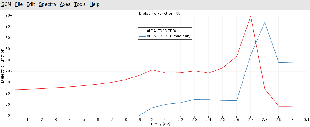
With respect to the accuracy of our calculation we can reproduce the main features of the dielectric function for this system. We cannot expect the spin-orbit splitting of the first transition at around 1.9 eV to 2.1 eV, since we don’t use Spin-Orbit Relativistic ZORA.