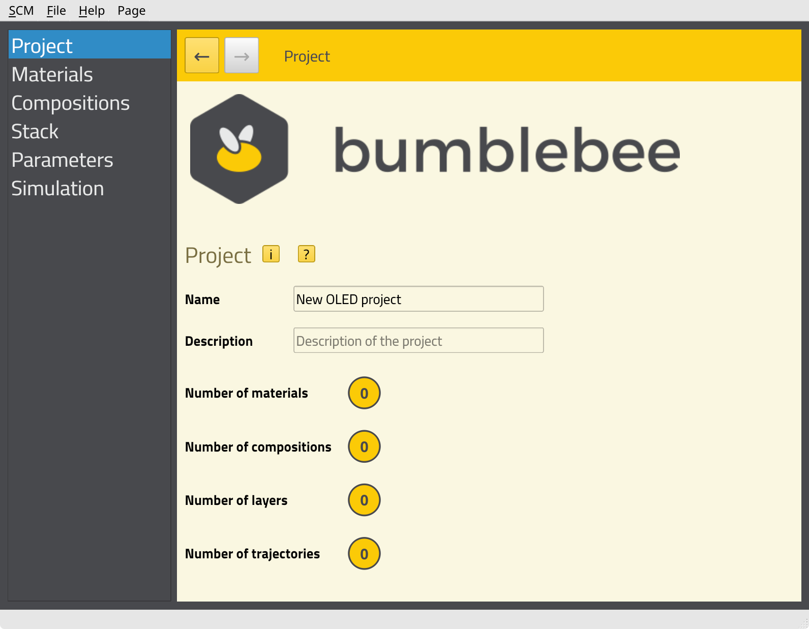
Multiscale modeling of OLED devices
Introduction
The Amsterdam Modeling Suite, together with Bumblebee, provides a fully integrated multiscale simulation platform for the digital screening and prediction of successful OLED materials and devices.
This tutorial teaches you how to:
AMS: Simulate physical vapor deposition to deposit thin films of organic materials: an emissive host-guest layer (EML) consisting of 95% CBP and 5% fac-Ir(ppy)3, a hole transport layer (HTL) of TAPC, and an electron transport layer (ETL) of TPBi.
AMS: Calculate the distribution of properties such as ionization potential, electron affinity and dipole moments for molecules in the film.
Bumblebee: Transfer the data to the Bumblebee kinetic Monte Carlo (kMC) code for OLED device simulations.
Bumblebee: Build an OLED stack from these virtual materials and perform a voltage sweep to calculate the J-V curve and investigate the roll-off in device efficiency at higher voltages.
It is recommended to run this tutorial with an HPC (compute cluster) system.
Optional: You can load results from the OLED material database to skip steps 1 and/or 2 and jump directly to the device-level modeling.
See also
Description of the methods in steps 1 and 2: OLED workflows documentation.
Description of the methods in steps 3 and 4: Bumblebee documentation.
The OLED workflows are developed and validated in close collaboration with the Eindhoven University of Technology
Step 1: Deposition of the materials
We want to generate morphologies of
the emissive host-guest layer (EML) of 95% CBP and 5% fac-Ir(ppy)3,
the hole transport layer of TAPC, and
the electron transport layer of TPBi,
Here, we show the first step of how to generate the EML morphology with physical vapor deposition. Depositions of the hole and electron transport layers are done in the same way.
 →
→ 
 on the right to go to the Model → OLED Deposition panel.
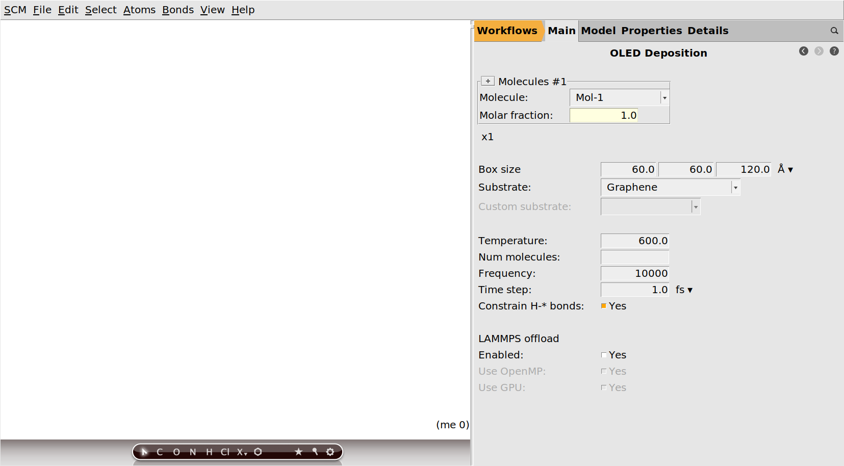
Import the CBP molecular structure
We need the 3D structures, including bonds, of the molecules we want to deposit.
Both CBP and fac-Ir(ppy)3 can be found through the search box in AMSinput, as can all other molecules from the OLED material database.
 .
.CBP and select CBP from the list.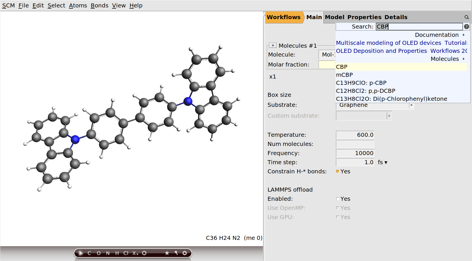
Fig. 50 The initial CBP molecule, after deselection and some rotation
If you want to deposit a molecule for which you do not yet have the 3D structure, you can
build it using the tools in AMSinput, or
copy-paste the SMILES string of the molecule (e.g. from PubChem) into AMSinput. This will try to generate a 3D structure using RDKit, which should work quite well for organic molecules.
Pre-optimize with GFN1-xTB
No matter how you obtain the initial structure, we recommend that you do a quick pre-optimization with the fast quantum-mechanical GFN1-xTB method.
 .
.If you loaded the CBP structure through the search box, the pre-optimization will not change much, since all molecules from the OLED material database have already been optimized with GFN1-xTB. In general this step is important though, as it will also update the bond orders to the ones calculated from the GFN1-xTB orbitals.
Check atom types
The deposition is done with the ForceField engine using the UFF4MOF-II force field. It will use the bonds and atom types as they are set up in AMSinput, so it is important to get them right at this point. We should therefore also check the atom types that will be used:

For CBP, the automatically determined atom types are fine.
Repeat for fac-Ir(ppy)3
We will now add the emitter molecule Ir(ppy)3 and define the composition of the host-guest layer.
 button to add a second molecule..
Irppy3 and select fac-Irppy3 from the list..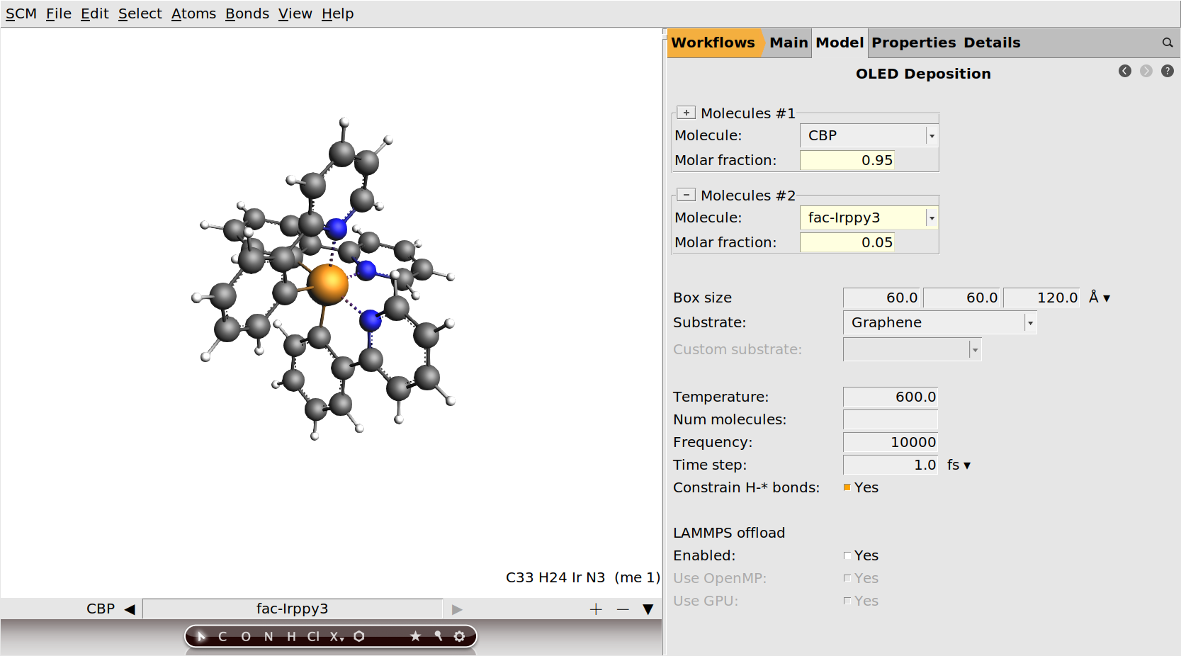
We will not change any of the deposition settings from their default values. By running with all default settings, the results we get should match those in the OLED material database.
Optional: Enable LAMMPS offload
Tip
You can significantly accelerate the deposition by enabling the LAMMPS offload option.
In order to do so, you must first
build LAMMPS on the system where you want to run the deposition.
ensure that the
lmpexecutable is available on your PATH
Then:
OMP package.GPU package.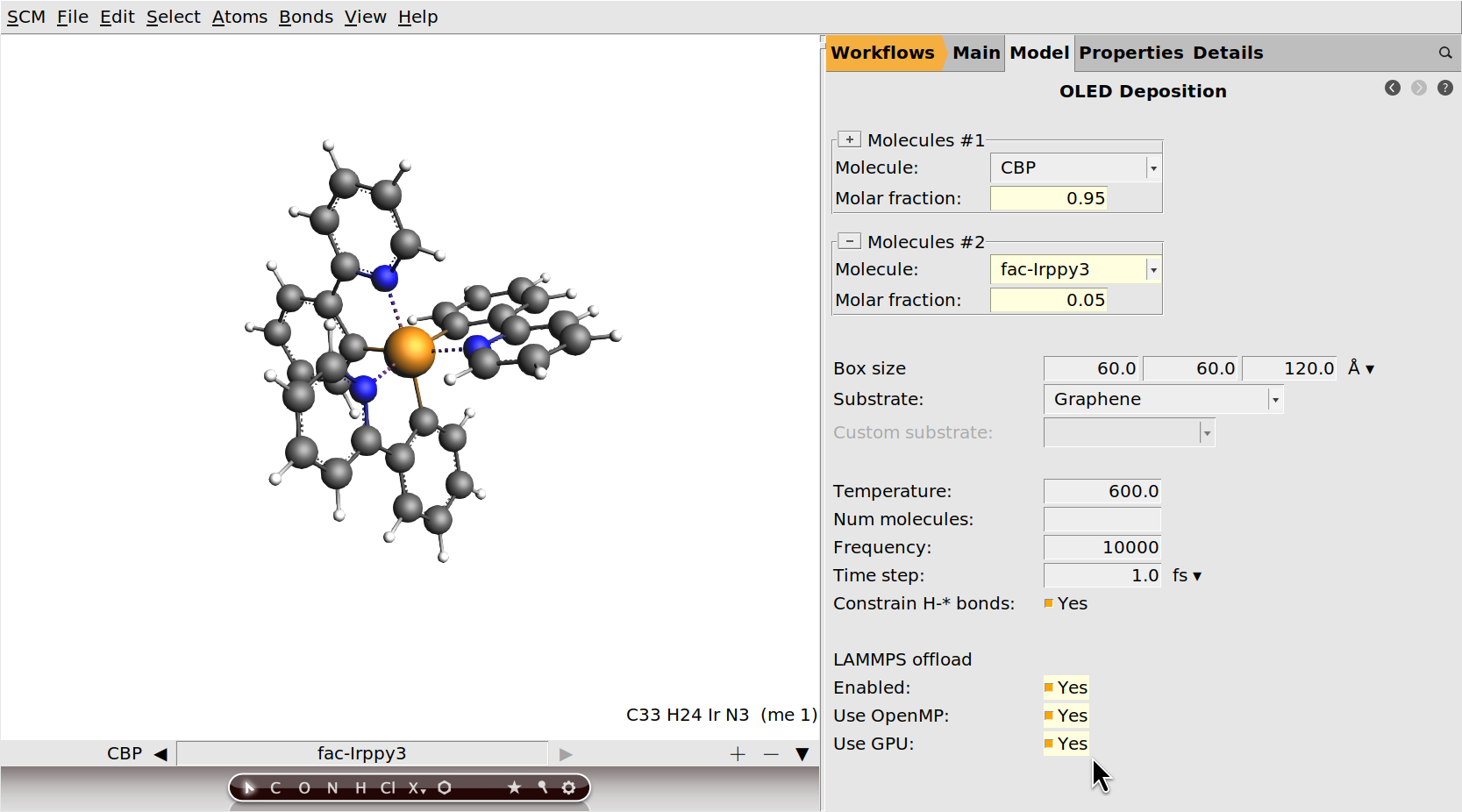
Run the deposition and monitor the progress
We are now ready to run the calculation.
EML_deposition.The first step in the deposition workflow is a DFT geometry optimization of CBP and Ir(ppy)3. This is done to determine the atomic charges that will be used for modeling the electrostatics with the force field. See the OLED workflows manual for more information.
You can also monitor the progress of the workflow in AMSmovie, which will open the latest or currently running job.
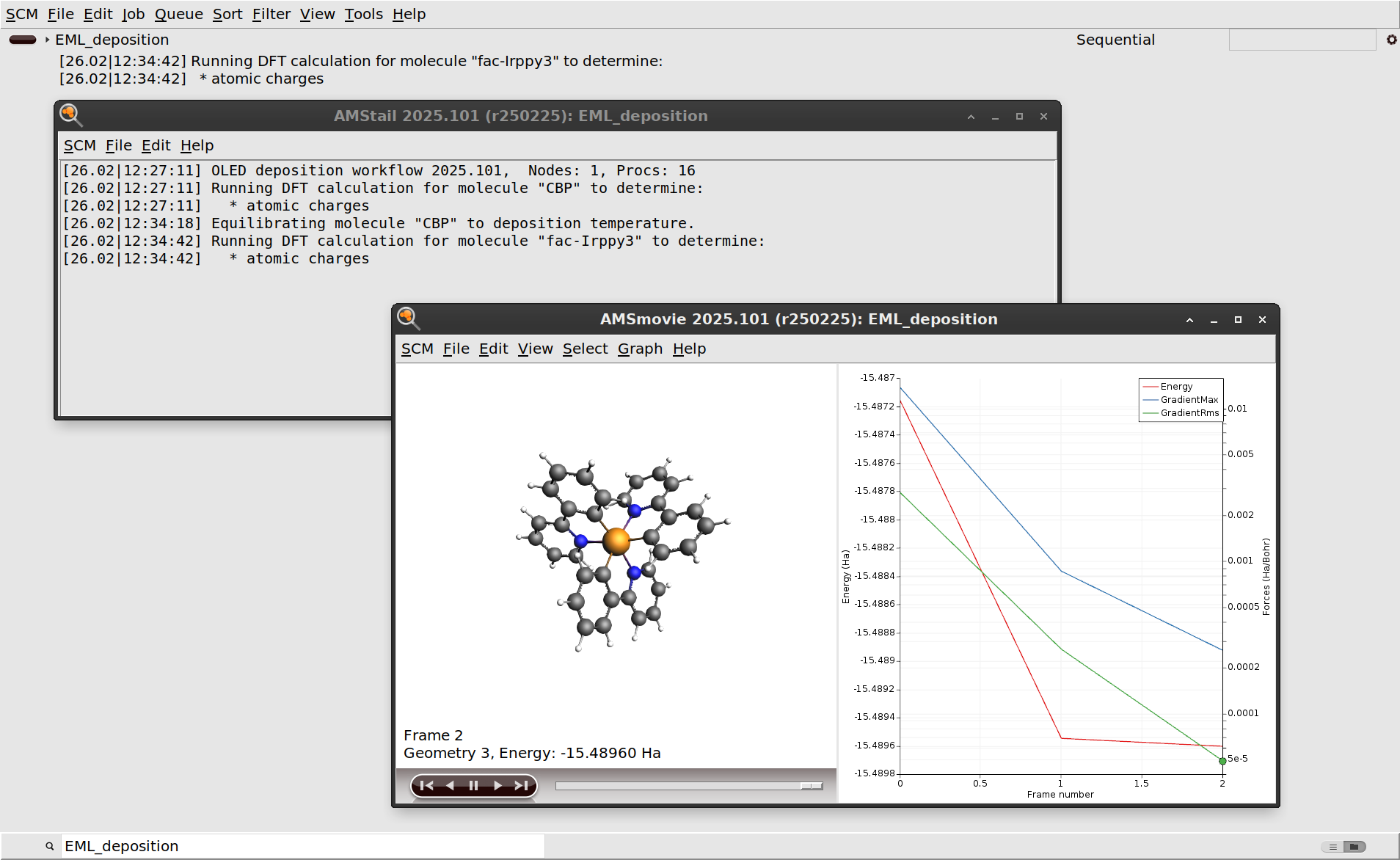
After the initial DFT calculations have finished, the molecules are equilibrated to the deposition temperature. At this point the workflow script will also print some information about the estimated number of molecules to deposit in order to grow a slab of the desired thickness.
After this, the actual simulated physical vapor deposition will begin.
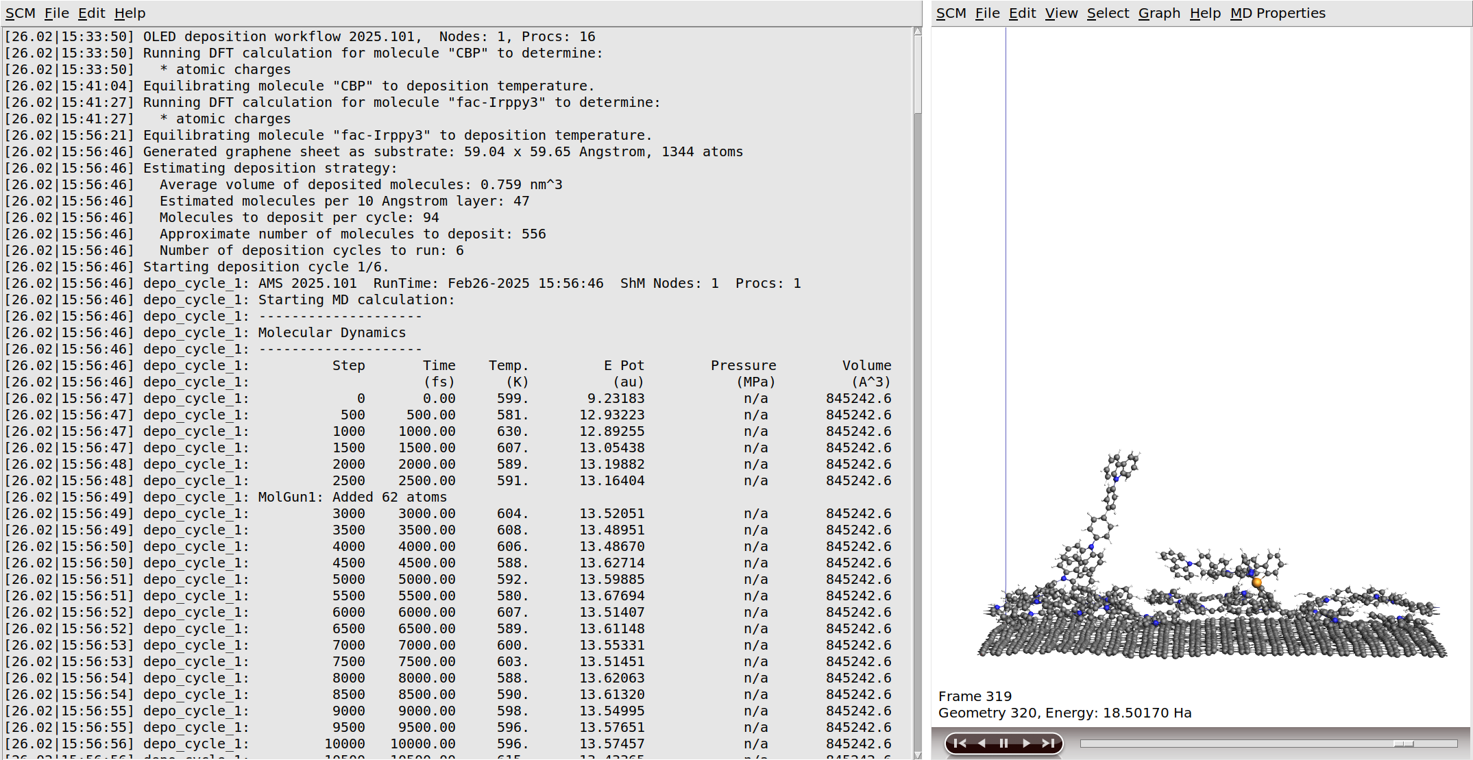
Growing a 120 Å layer in the simulated physical vapor deposition will take a while:
With LAMMPS offload enabled and a capable GPU: < 1 day.
With LAMMPS offload, but without a GPU: ~2 days
Not using the LAMMPS offload: significantly slower
We therefore recommend running these jobs using a remote queue. If you have access to a compute cluster, but have not yet set up remote queues for it, we recommend doing this before running real depositions. You can find instructions on how to set up remote queues in the installation guide and the AMSjobs manual.
If you monitor the logfile of the deposition for a while, you will see that the entire deposition is split into a number of cycles. This is done to improve computational efficiency, as it focuses the simulations on the region containing the growing surface. Details can be found in the OLED workflows manual. Once the required film thickness is achieved, the entire system is annealed down to room temperature and then completely frozen in a geometry optimization. The full process can be seen in the video on the right.
Output morphology: morphology.in
The output of the deposition workflow is described in detail in the manual.
The morphology.in file contains the optimized morphology.
If you do not want to wait for the deposition to finish, you can also find the morphology of 95% CBP + 5% Ir(ppy)3 from this tutorial
in the OLED material database as
host+guest/CBP+fac-Irppy3/morphology.in, oravailable for download
CBP+Irppy3_morphology.in.
The .in file can be opened with AMSinput.
Deposition of hole and electron transport layers
At this point you can either deposit the hole transport layer (TAPC) and electron transport layer (TPBi) yourself by repeating the instructions above, or grab the finished morphologies from the pure folder in the OLED material database .
Step 2: Calculation of material properties
Once we have obtained the morphology, we can use it to run the OLED properties workflow and obtain material properties such as ionization potential and electron affinity.
Import morphology
→ on the right to go to the Model → OLED Properties panel.The OLED properties workflow has a number of settings, which we will mostly leave at their default values in this tutorial. The data from the OLED material database has been generated with the default settings, so we will obtain results that can directly be compared to the materials from the database.
The only real input we will need to provide is the morphology itself.
If you did not run through the first part of this tutorial, we suggest you download the 95% CBP + 5% Ir(ppy)3 morphology now or take it from the database, which you can open by clicking the Import button on the right panel.
morphology.in (or CBP+Irppy3_morphology.in) file for 95% CBP + 5% Ir(ppy)3.Select subset of molecules
Be default, the workflow would calculate the molecular properties for all ~500 molecules in the morphology. This yields the best statistics, but is also quite computationally expensive. Since we really only need good mean values \(\bar x\) and distribution widths \(\sigma_x\) (standard deviations) as input for Bumblebee, it is sufficient to just select a (random) subset of molecules for each species. After all, the standard error of the mean \(SE_{\bar x}\) can be estimated from the standard deviation \(\sigma_x\) and sample size \(N\):
Taking typical values of \(\sigma_\text{IP/EA} = 0.1~\text{eV}\) for ionization potential and electron affinity and a sample size of \(N = 50\), gives an error of the mean of \(SE_\text{IP/EA} < 0.015~\text{eV}\). This is far below any methodological error in these workflows, and therefore completely sufficient for providing input to Bumblebee.
Since Bumblebee does not yet use the transfer integrals calculated by the OLED properties workflow, you may consider disabling their calculation. (Transfer integrals are only calculated between dimers of the selected subset of molecules. With our small sample size they would be relatively few and inexpensive, and skipping them does not make a big difference.)
50.None.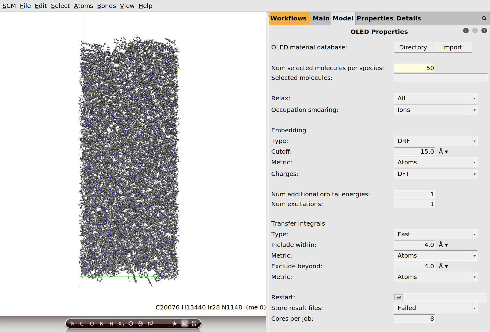
This is all the setup we need. We can now save and run the job.
Run the OLED Properties workflow
EML_properties.The OLED properties workflow is computationally very expensive, and it is not practical to run it on your local machine: we will need to use some HPC facilities to run these jobs. You can do so from AMSjobs by using a remote queue. You can find instructions on how to set up remote queues in the installation guide and the AMSjobs manual. The OLED properties workflow consists of many independent chains of calculations for the individual molecules in the morphology, making it scale very well up to hundreds of CPU cores.
Note
Multi-node OLED properties jobs are currently only supported for SLURM-based clusters. For other batch systems, you will be limited to running the jobs on a single node.
Once you have configured a suitable remote queue for your job, we are ready to run.
EML_properties job.Monitor the progress and results
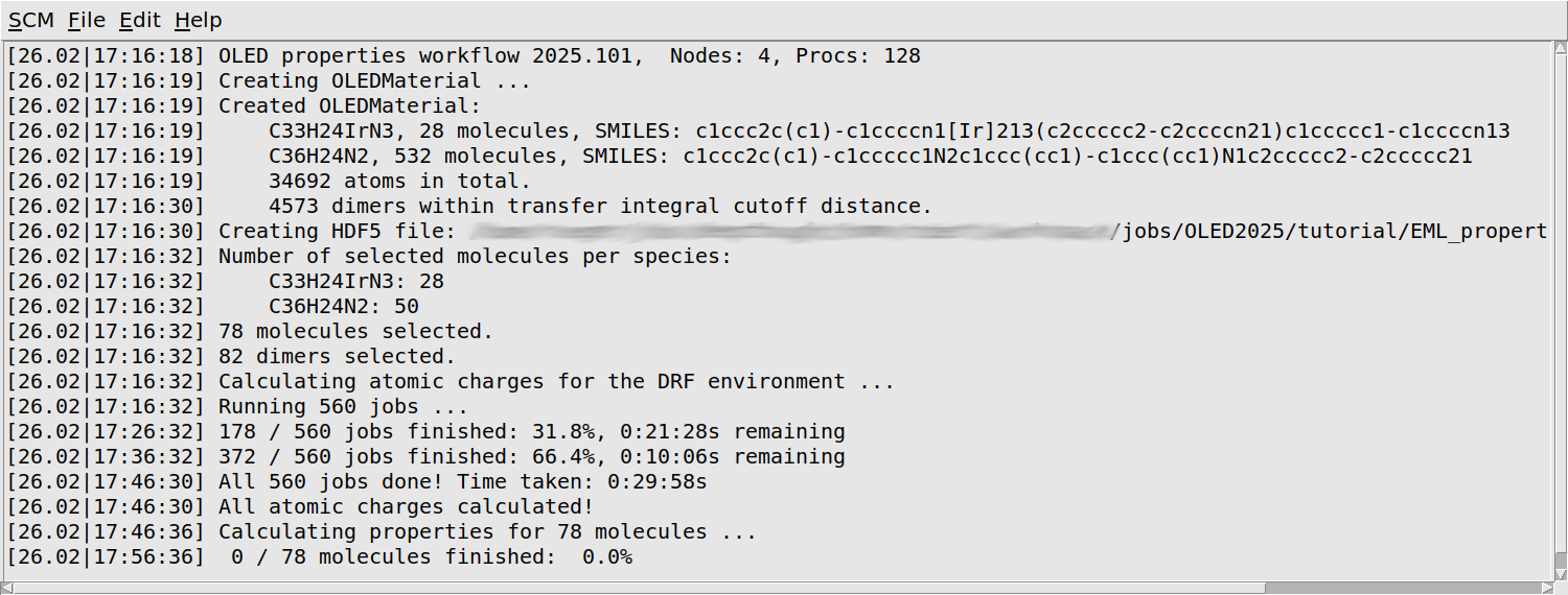
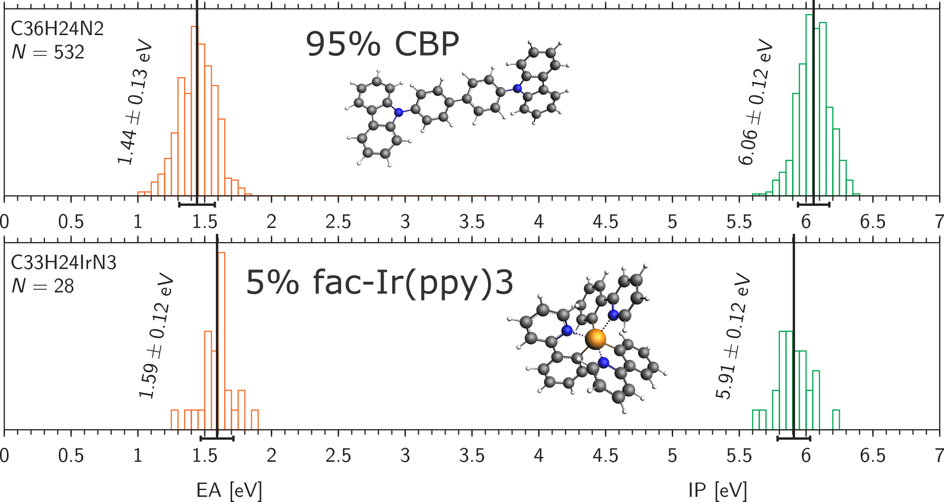
You will first see some information about your morphology printed: the number of molecules of each separate species, as well as the total number of atoms, and the number of dimers considered in the calculation of the transfer integrals.
The workflow script will periodically print a progress update. You will see that it loops over all molecules twice: first to quickly calculate the atomic charges that will later be used as the environment, and then again to calculate the properties of each molecule in its environment. Finally there is a loop over dimers of neighboring molecules, which calculates the transfer integrals. Depending on the machine you are running on, it may take around a day to finish all calculations.
View the finished OLED Properties results
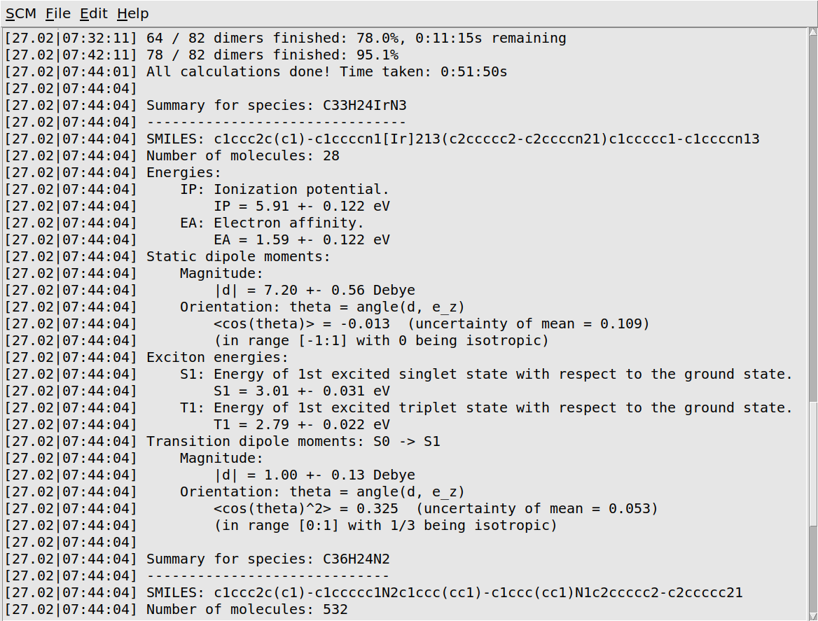
When the job has finished, it will print a quick summary of the most important results. The workflow script will also produce small HDF5 and YAML files. The HDF5 file contains data for all the individual molecules. It can be opened in AMSview or analyzed with our Python environment. The YAML file contains only a summary of the distribution means and widths. We will later use it to import these results into the Bumblebee GUI modules.
If you do not want to wait for the calculation to finish, you can download the files here (HDF5) and here (YAML) or take them from the OLED material database, where it is stored as host+guest/CBP+fac-Irppy3/properties.{hdf5,yml}.
You will be greeted by a view of a box that is filled with disconnected spheres. Note that these spheres do not represent atoms, but individual molecules from the morphology. The spheres representing host CBP and guest Ir(ppy)3 molecules have a different color. We can visualize the properties we calculated via the Properties menu in the top bar.
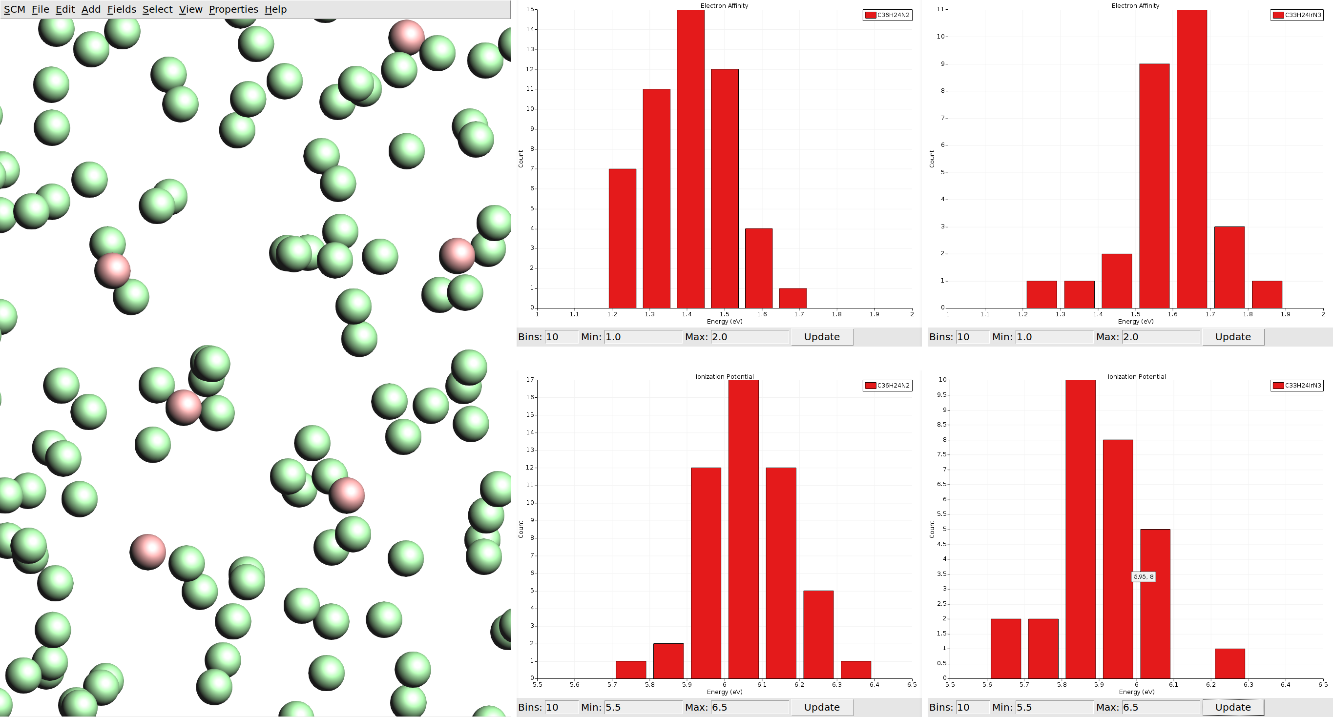
We can also visualize vector properties as arrows overlaid onto the spheres, and plot histograms of the vector magnitudes as well as angles against the z-axis (the growth direction of the thin film in the deposition).
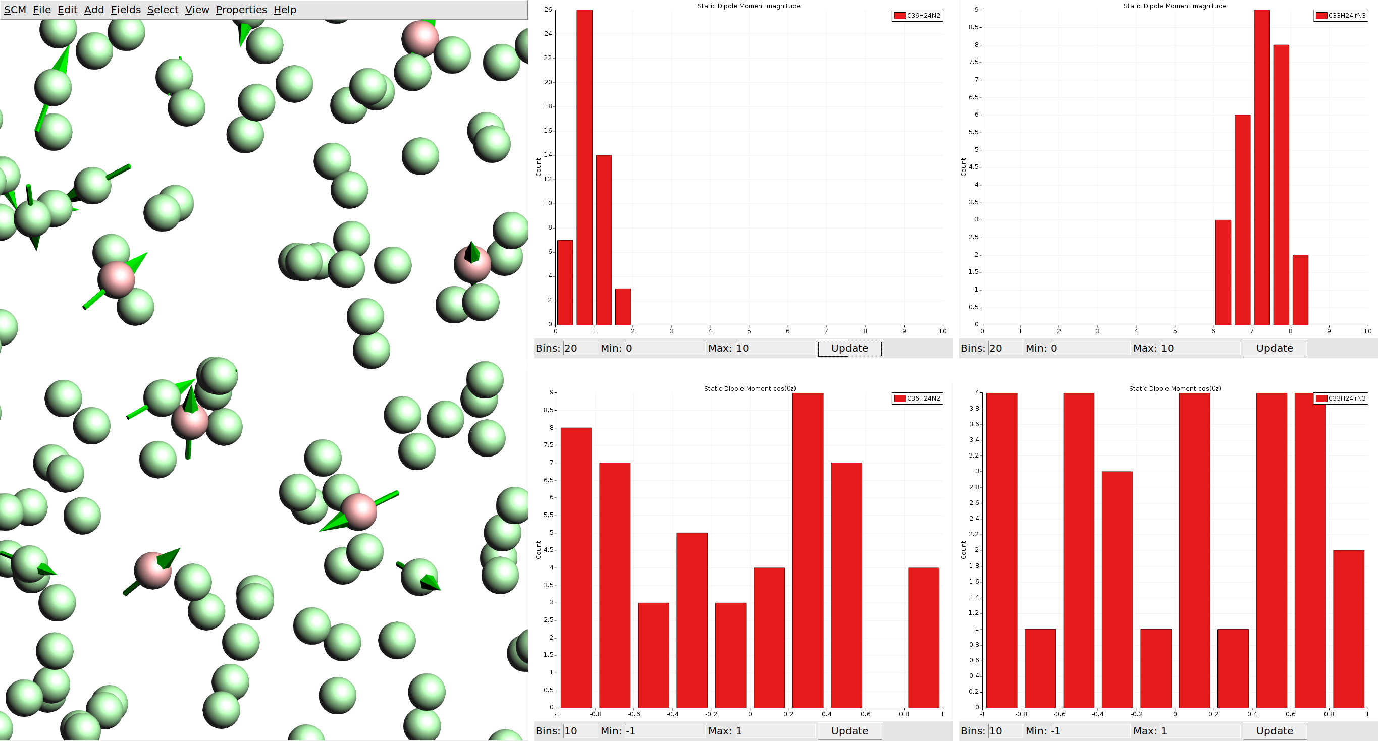
With the limited number of molecules we calculated per species, our statistics are not good enough to say much about a possible anisotropy of the dipole moments. If such spatial properties are desired, it is recommended to run calculations on all molecules in the morphology. (For comparison you can load the HDF5 files from the material database, which include data for all molecules.)
Detailed analysis of the data from the HDF5 file is best done from Python. See the manual section for details.
Step 3: Import materials for Bumblebee device simulations
The layer morphologies (and their properties) can be imported into the BBinput GUI module for setting up Bumblebee jobs. The layers can then be combined into a microscale OLED stack, representative of a real device. Bumblebee allows the user to perform 3D kinetic Monte Carlo simulations of the electron transport through the stack. This provides detailed information on the efficiency of the OLED device. We can use this information to identify loss processes and find desirable material parameters to improve the stack design.
Compositions
We will start by importing the three layers created during the previous step. If you skipped the property calculations, you can obtain the necessary files from the OLED material database, or through the links below.
See also
95% CBP + 5% Ir(ppy)3Host-guest emissive layerTAPCHole transport layerTPBiElectron transport layer
Open the BBinput GUI module through the SCM menu.
Click File → Import → Composition in the top menu to open up the Import compositions window.
We will start by importing the composition of the emissive layer.
Clicking the Open file button will bring up a dialog box where you can browse to the .yml file of the layer materials.
If you ran the properties calculation earlier, you will find it as properties.yml in the .results folder of that job.
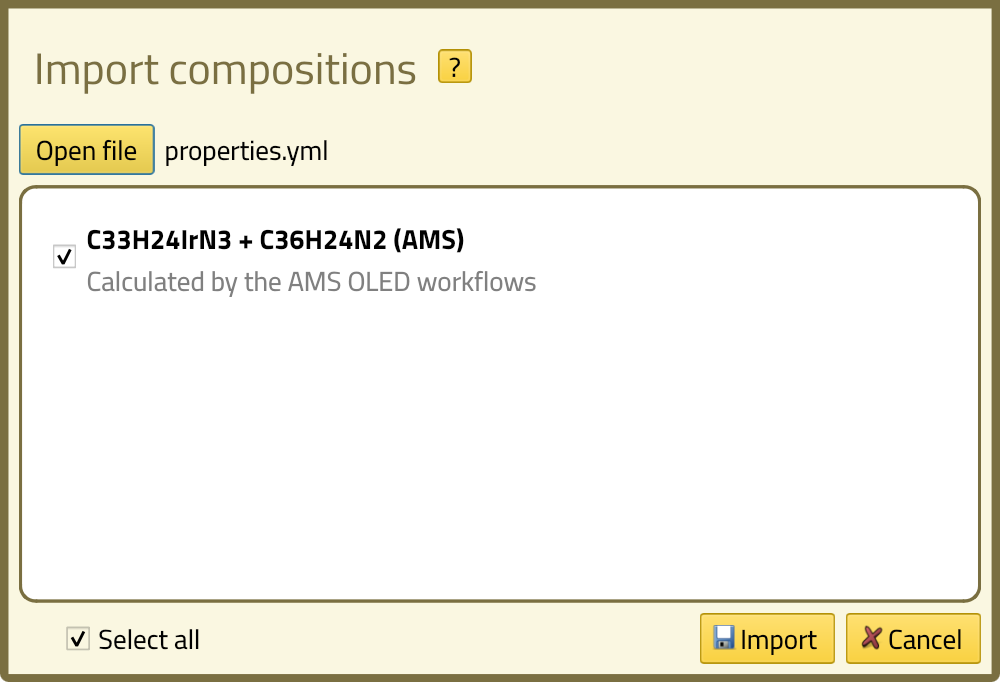
If a loaded file contains more than one composition, we can select which ones to import here. The file we loaded now only contains a single composition and it is already selected, so we can just click the Import button. You will see the new composition appear in the list. Click on the name of the composition to view the details.
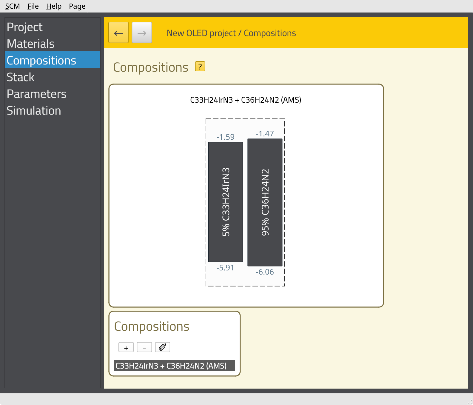
Perform this process for all three layers: CBP-Ir(ppy)3, TAPC and TPBi.
Step 4: Set up and run an OLED stack simulation
Materials
Importing the compositions has also created the corresponding materials. You can view the material properties on the Materials page.
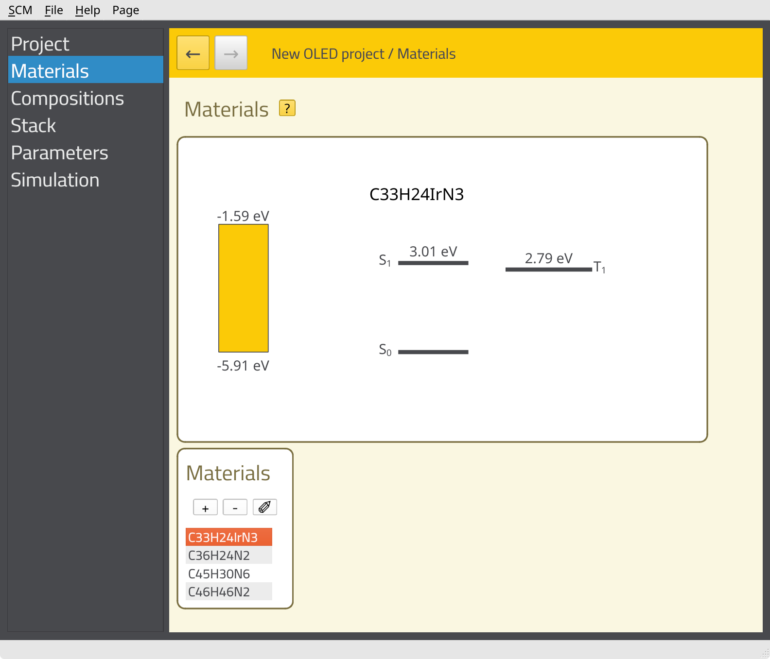
At this point, we do not yet have the emissive characteristics of Ir(ppy)3 included in the material properties. While the rates for radiative emission, non-radiative emission and intersystem crossing can be calculated using AMS, these parameters are not included in the OLED properties workflow. Instead, they are typically calculated for single molecules. Environmental effects and amorphous disorder for the rates are then estimated by Bumblebee based on the morphology data.
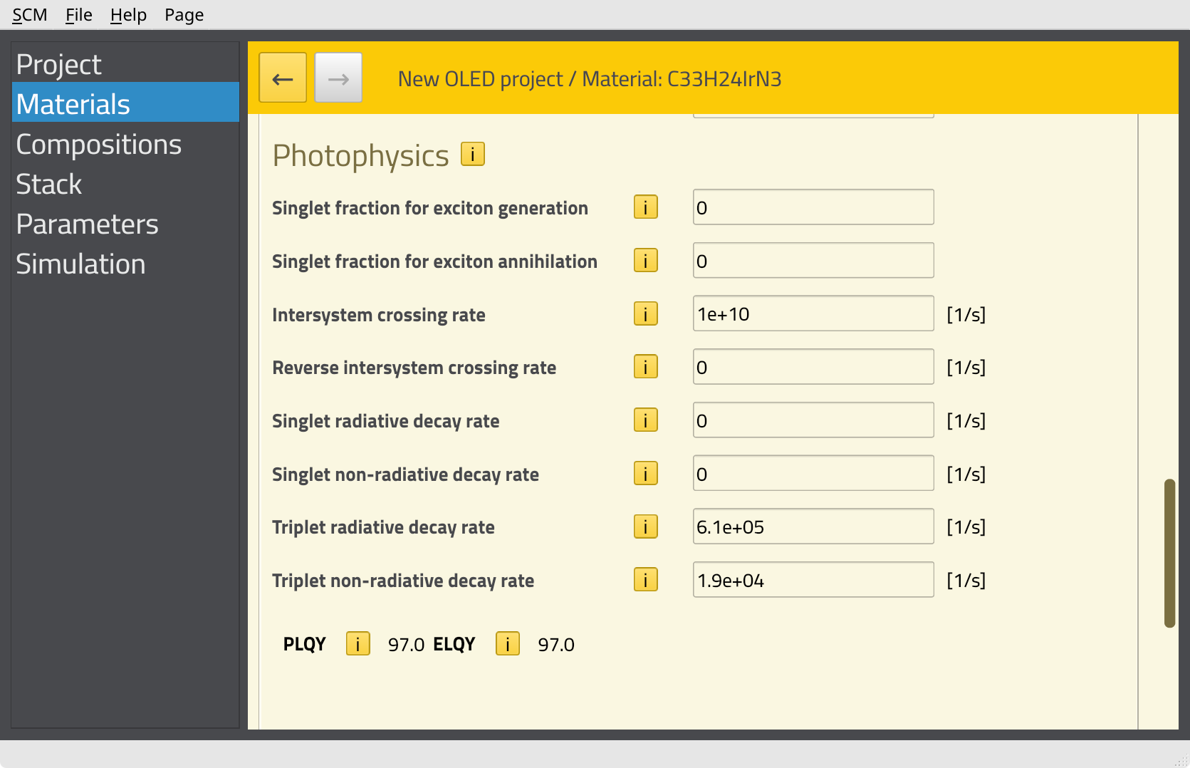
Photophysics: Specify decay rates for Ir(ppy)3
In order to include emission from Ir(ppy)3 in the simulation, we need to specify the decay rates on the Materials page. We will use the experimental parameters provided in the Bumblebee tutorials.
610000 s-119000 s-11e10 or 10000000000.0You should see an estimated PLQY of 97% (based on a rate equation model). This provides an indication of the molecular emitter efficiency.
Stack
We will create an OLED stack containing the hole transport layer, emissive layer and electron transport layer.
HTL by clicking the field in the Name column.EMI containing 30 nm of C33H24IrN3 + C36H24N2.ETL containing 20 nm of C45H30N6 (TPBi).The energy level diagram of the stack will be shown at the top of the page.
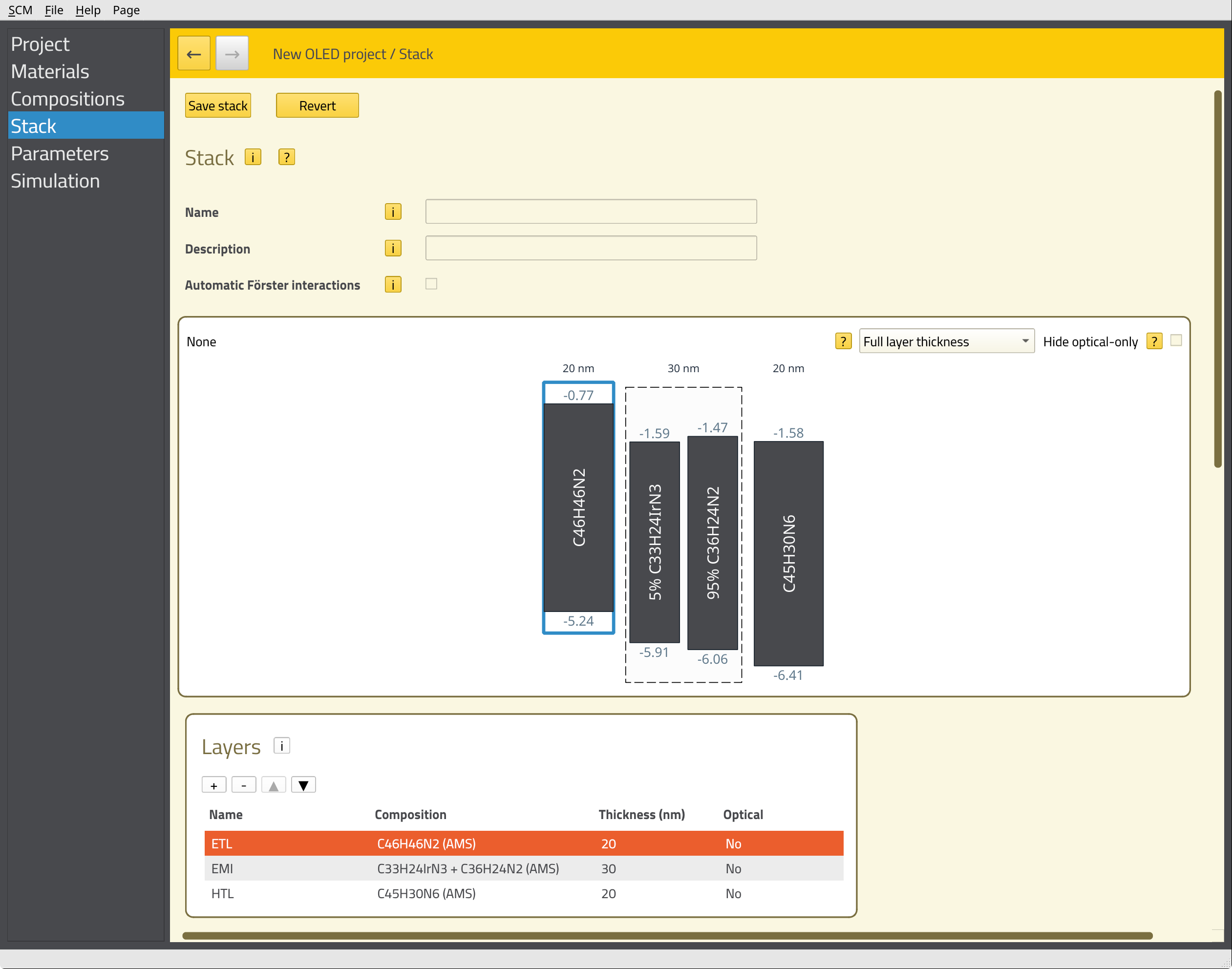
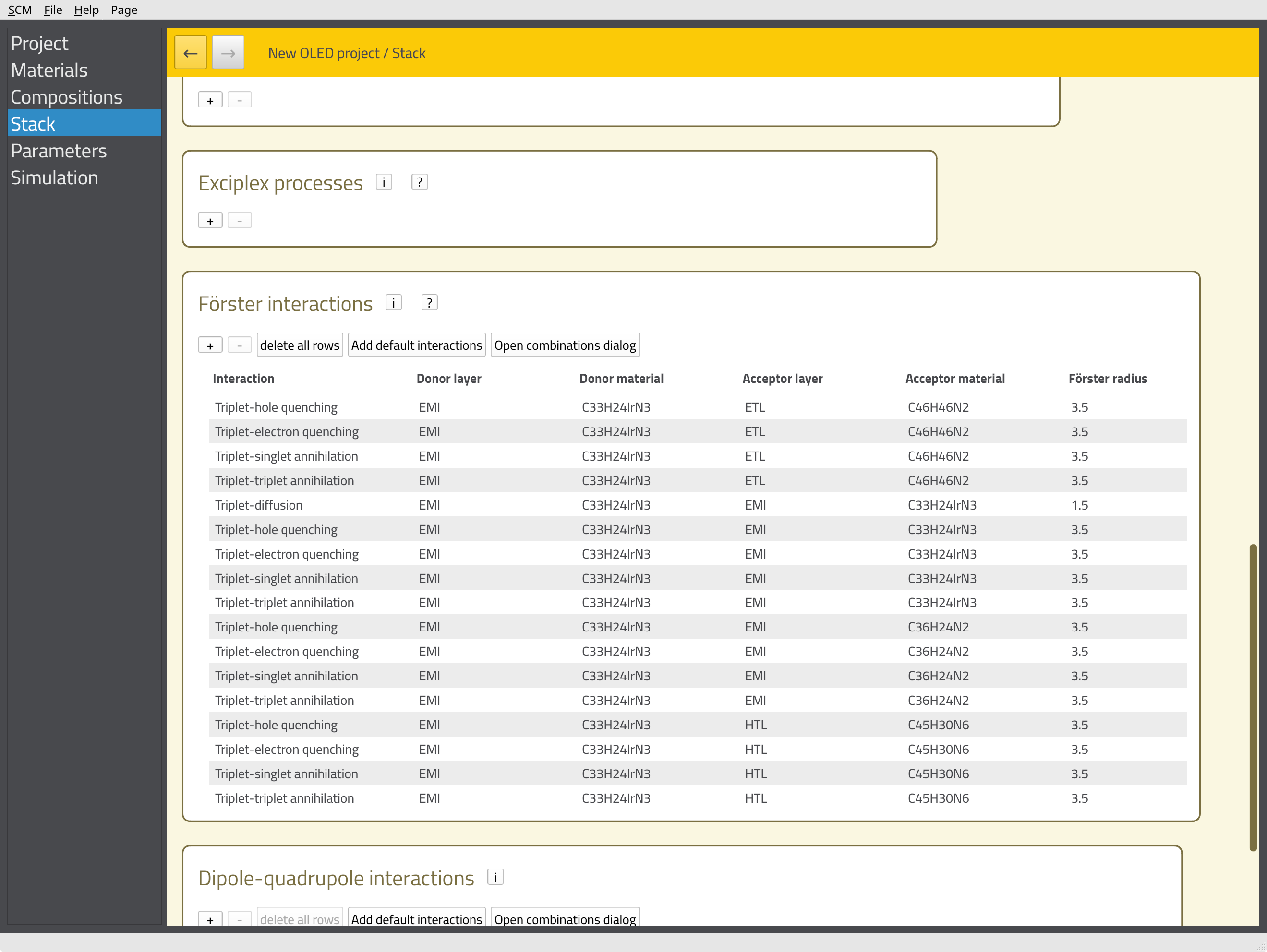
We can now define additional processes for our stack, such as degradation mechanisms or exciplex interactions. Because we are using a phosphorescent emitter, we want to include the Förster interactions here. We will have Bumblebee automatically generate these interactions for our stack by scrolling down to the Förster interactions section and clicking the Add default interactions button. This populates a table with pair-wise interaction parameters for the materials in our stack.
This concludes the setup of the stack. Scroll to the top of the page, and click the Save stack button.
Parameters & Simulation
Technical details of the job are set up on the Parameters page.
1000000000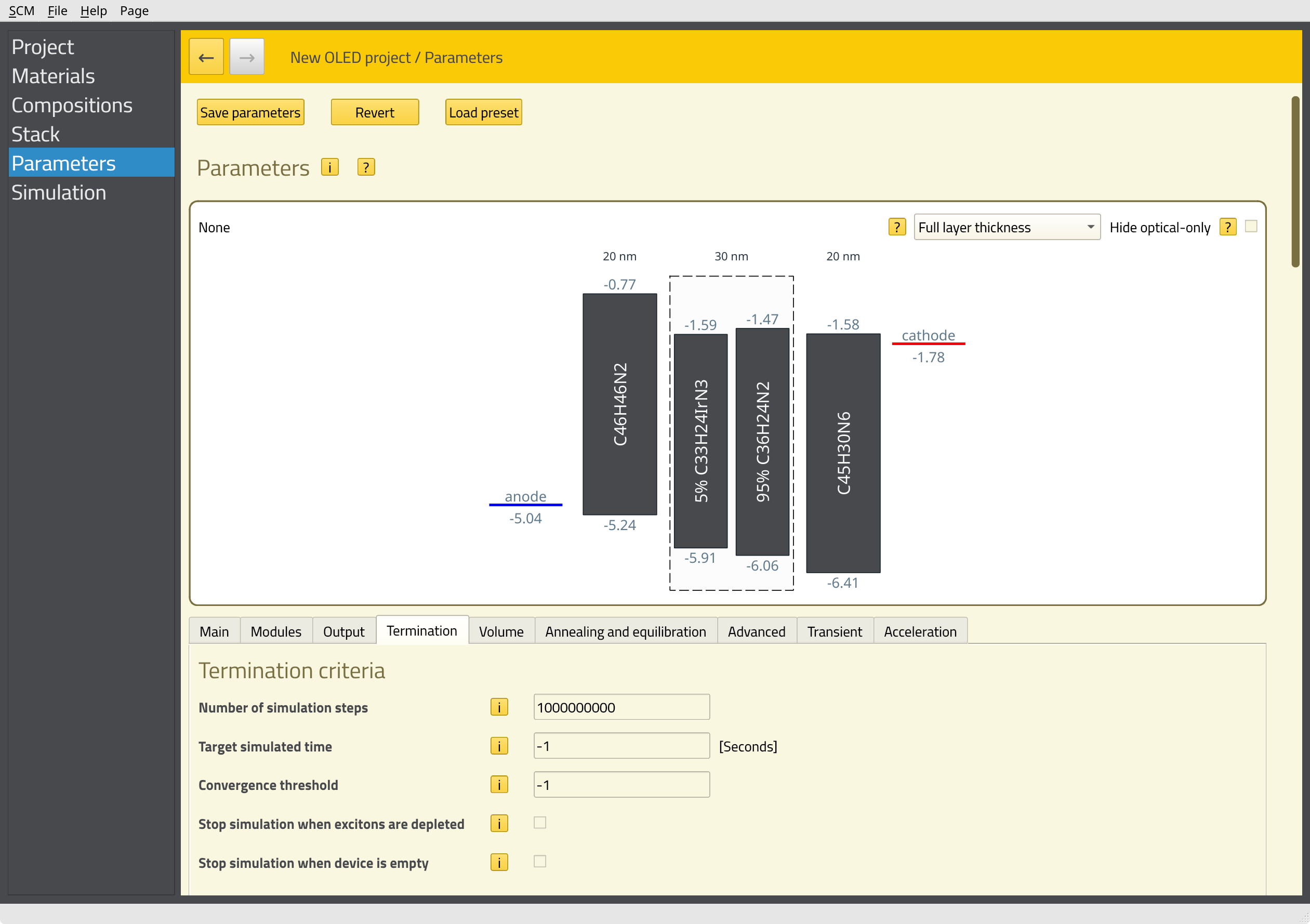
In this tutorial, we want to perform a voltage sweep. This means multiple kMC simulations will be started at different voltages in order to construct the J-V curve for the device. Later, we can analyze the processes inside the stack at each of these voltages. This parameter sweep is set up on the Simulation page.
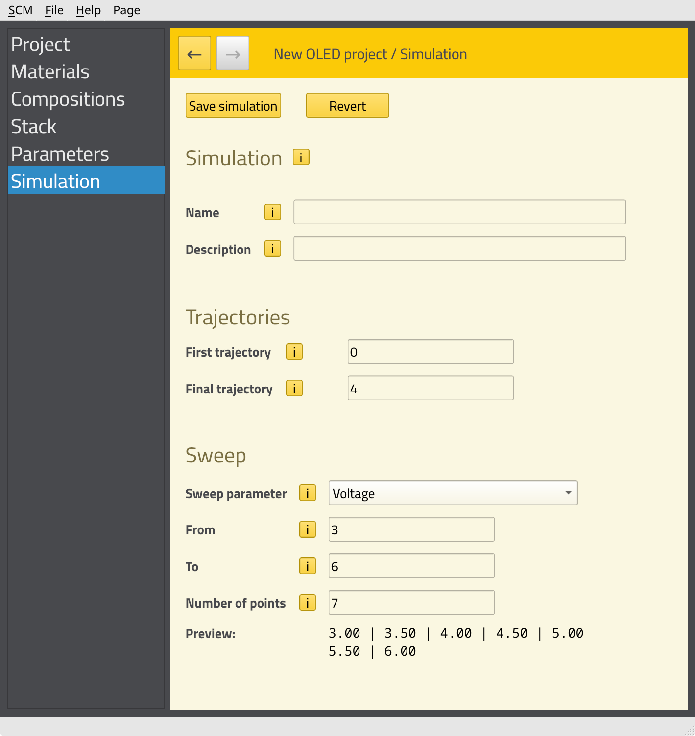
This concludes the setup of the job. Click File → Save and give the job an appropriate name. AMSjobs should automatically open to show the job.
Running and monitoring the job
Bumblebee jobs can take a long time to run. We therefore suggest you run them through a remote queue. If you have access to a compute cluster, but have not yet set up remote queues for it, we recommend doing this now. You can find instructions on how to set up remote queues in the installation guide and the AMSjobs manual.
Note
Ideally, the number of queue tasks should match the total number of trajectories. In this tutorial, we have 7 sweep points with 5 trajectories each, so 35 trajectories in total.
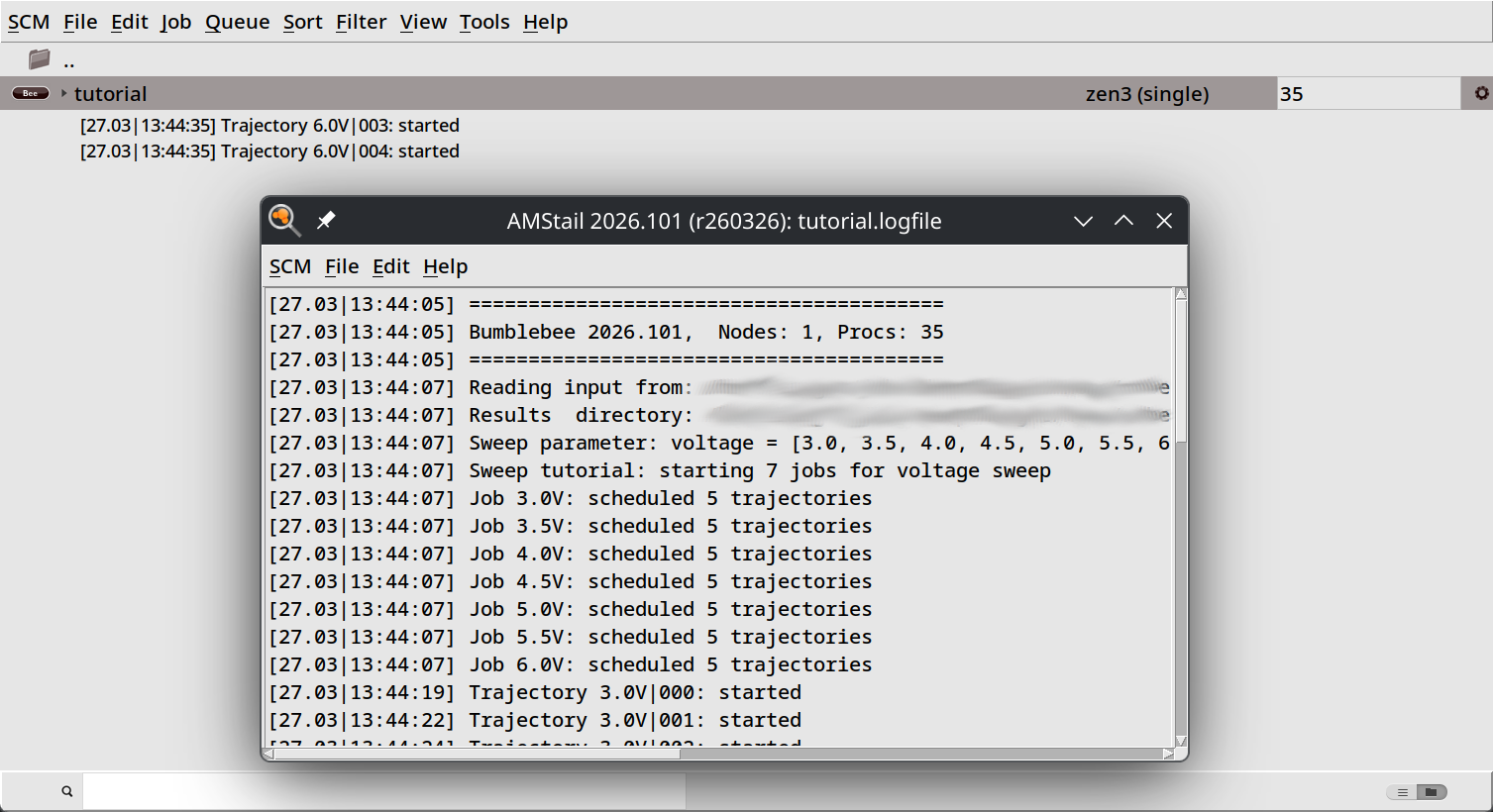
Give your job a few minutes to fully start up. You can then monitor the progress of the simulation using the BBresults GUI module.
6.0V point to visualize the convergence of the Monte Carlo method at that voltage.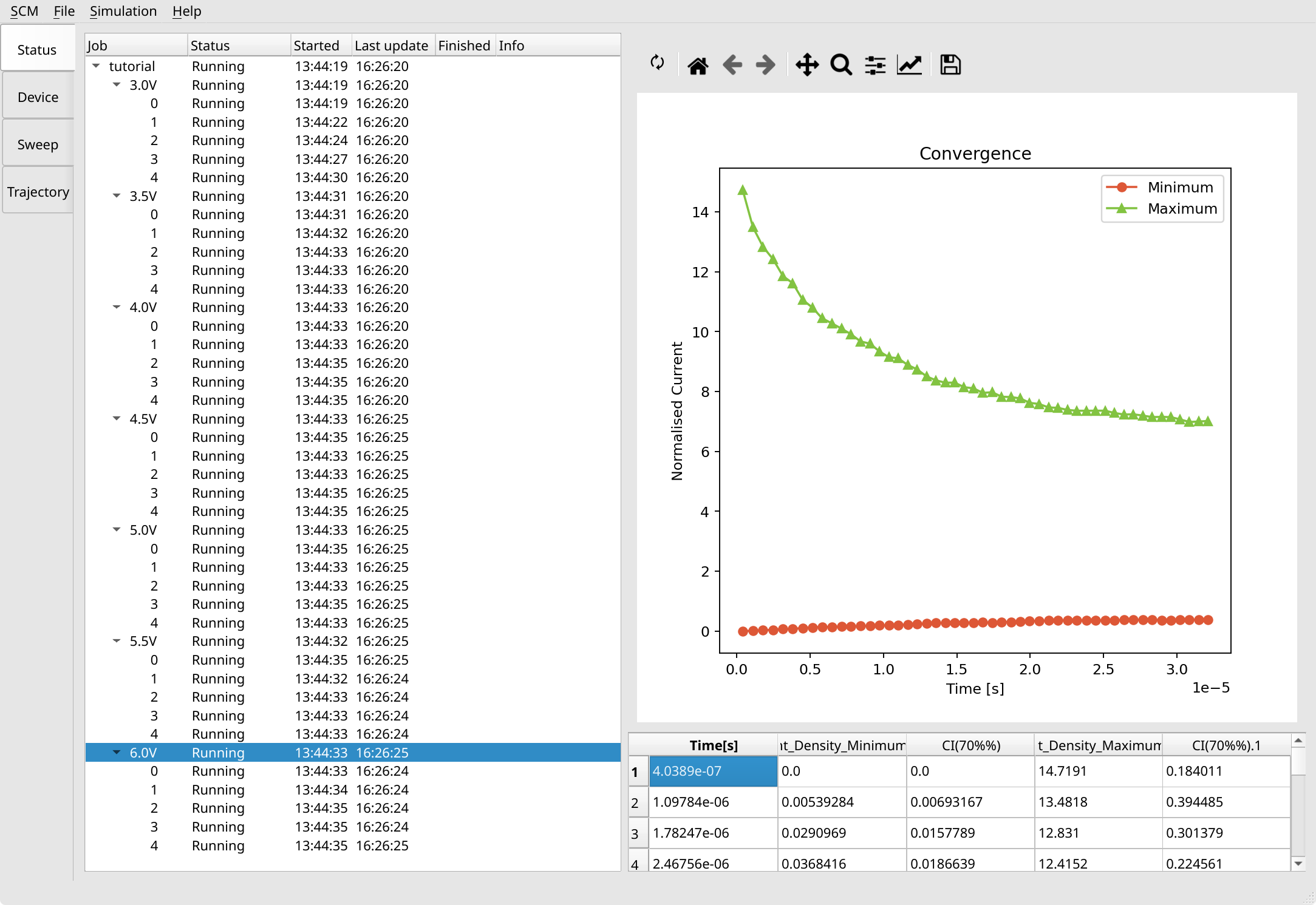
You will notice that calculations at higher voltages are faster to converge. Once convergence is reached, sweep points (and also individual trajectories) can be stopped by right clicking them and selecting Request stop, or via the Simulation menu entry at the top.
Analyzing the results
We can analyze the results of our calculation through the report tabs on the left of BBresults, just below the Status tab. There are three kinds of reports:
The Trajectory reports provide details on individual trajectories such as morphologies and event statistics.
The Sweep reports provide details for each single point calculation by averaging over the trajectories.
The Device reports summarize results from multiple single-point calculations to see how the OLED performance changes under various conditions.
Note that not all reports may be available for jobs that are still running.
We performed the same simulation using experimental parameters as part of the Bumblebee tutorials. Close agreement is found for the device behavior predicted by the OLED Workflow, despite there being quite some differences in the actual parameter values. This is caused by a favorable cancellation of errors, as shifts in the energy levels are compensated by changes in overall mobility.
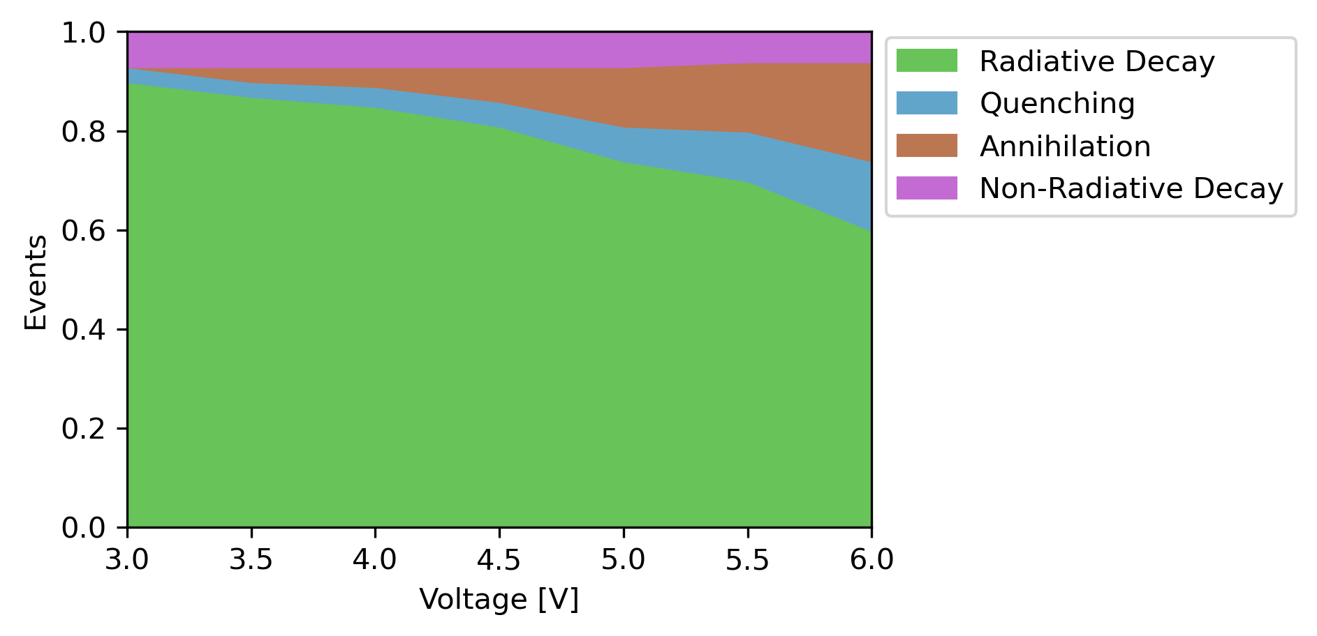
Digital OLED design
In our results, we have seen how the primary losses in the device originate from exciton-exciton annihilation. We could now go and make changes to the stack design to see if this can improve the device efficiency. Here, we can make use of various predefined materials in the Bumblebee OLED database (accessible from the File → Import → Material menu), which were obtained both through experiment and simulations.
Alternatively, we could make modifications to the material parameters ourselves in order to find idealized OLED molecules. These materials can be used in combination with e.g. molecule screening in AMS to help discover new materials through inverse design.
Consult the Bumblebee manual for additional examples on the various simulation options and optimization tools provided in Bumblebee.