Electronic transport in a carbon nanotube
See also
In this tutorial we will be modeling the electronic transport through a carbon nanotube using the NEGF formalism.

Setting up the calculation
The simulation in this tutorial can be performed with either the DFTB engine or the BAND engine. DFTB is computationally faster than BAND, but the results will generally be less accurate.
- Start up AMSinput1. Switch to DFTB:
 →
→  2. Select Task → NEGF3. Select Model → SCC-DFTB4. Click on the parameter directory folder and select DFTB.org/3ob-3-1

- Start up AMSinput1. Switch to BAND: →
 2. Select Task → NEGF

Note
In this tutorial we use the Non self consistent NEGF method of BAND. This method represents a computationally cheap alternative to the more sophisticated self consistent method, but it can only be used for zero-bias calculations. See the BAND-NEGF Documentation for more details.
Next, we switch to the NEGF panel where we can set up the geometry of our system and specify various NEGF calculation parameters:
- Click on
 next to Task: NEGF to switch to the NEGF panel (or click on Model → NEGF)
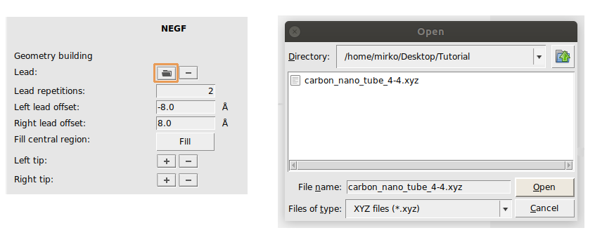
We first need an .xyz file defining our lead, that is, a carbon nanotube:
- Click
hereto download the .xyz file carbon_nano_tube_4-4.xyz
Now import the lead:
- 1. Click on the folder icon next to Lead: this will prompt a file dialog window2. Open carbon_nano_tube_4-4.xyz (the .xyz file you just downloaded)3. Set Lead Repetitions to 2
Note
The leads cannot be directly modified in the molecule-editing area. In the next tutorial we will show how to create a leads.
We now need to define our central region. In this tutorial, the central region consist of a nanotube (same as in the lead). We can easily fill in the central region with lead-material with the Fill central region option:
- 1. Click on Fill2. Enter 2 in the prompted dialog window and click on OK

This concludes the geometry-building part of a NEGF calculation. Your system should look like this:

From the NEGF panel we can change other parameters of the NEGF calculation, but in this tutorial we will use the default values.
Run the calculation and visualize the results
We are ready to run the calculation:
- Click on File → Save as…Run the calculation with File → RunWait for the calculation to finish
The results can be visualized with AMSspectra. To start up AMSspectra:
- Click on SCM → Spectra…
Here you can visualize:
- Transmission function \(T(E)\)
- NEGF-DOS (density of states)
- Current v.s. Bias Potential (computed from the the zero-bias Transmission function)
- In AMSspectra, click on Spectra → Transmission / Transmission+DOS / Current
Note
Energies are relative to the Fermi energy of the lead, i.e in the picture below, 0 eV corresponds to the Fermi energy of the nanotube (first simulation in Simulations work flow)
This is the computed transmission function of our nanotube:

