Closing the band gap of a 2D semiconductor with an electric field
This tutorial focuses on a monolayer of Molybdenum disulphide MoS2, because this material is of interest for transistors, in particular the switching to and from a conducting state. It is based on a CECAM workshop exercise.
Create the MoS2 monolayer
You can use the MoS2 monolayer from our database, follow step 1 of the MoS2 response tutorial.
Analyze the DOS and band structure
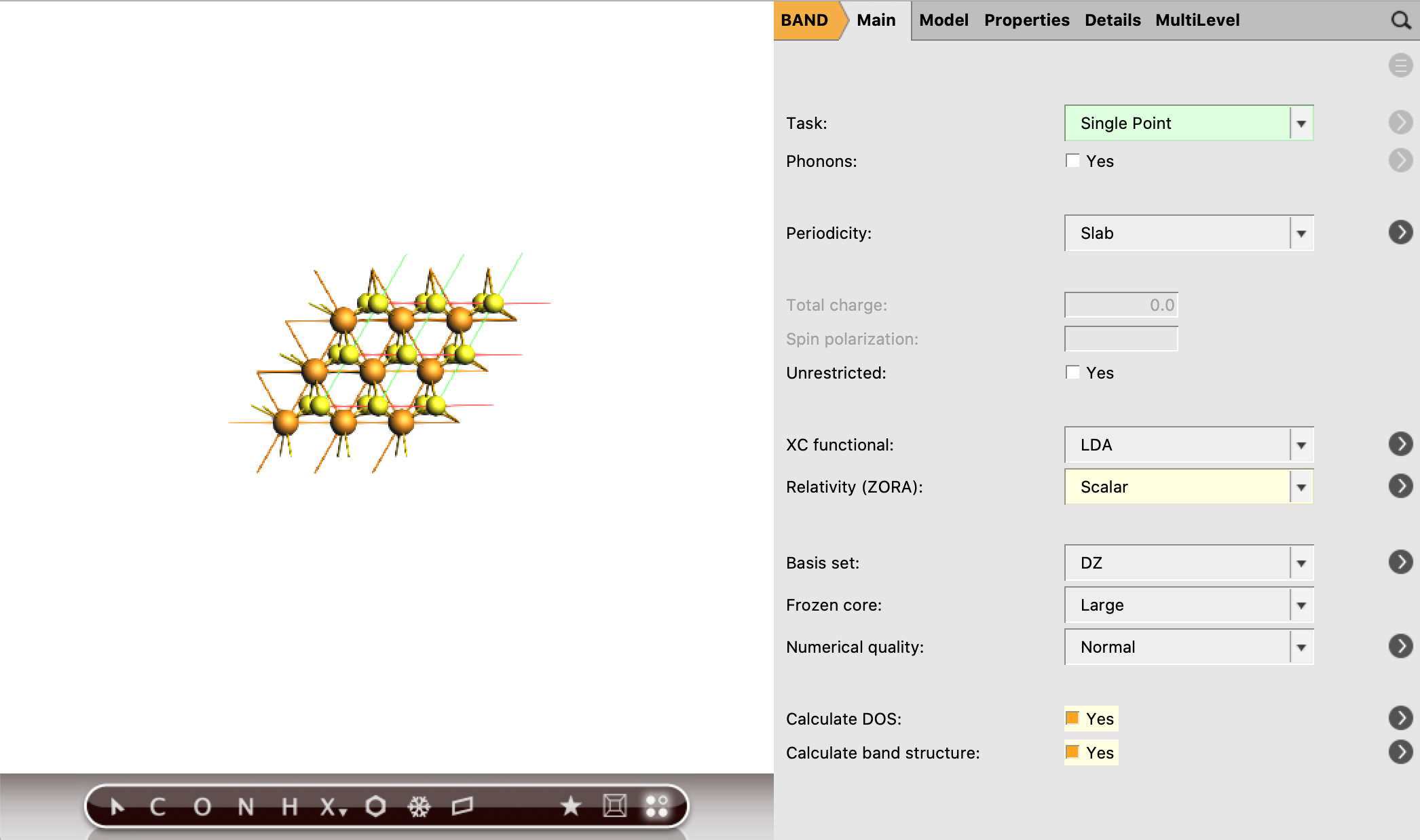
- 1. Select Relativity (ZORA) → Scalar in the Main menu2. Tick the Calculate DOS box3. Tick the Calculate band structure box4. Run the calculation (File → Run)
After the calculation is finished, the band structure can be visualized.
- 4. Open the band structure by selecting SCM → Band Structure in the menu bar
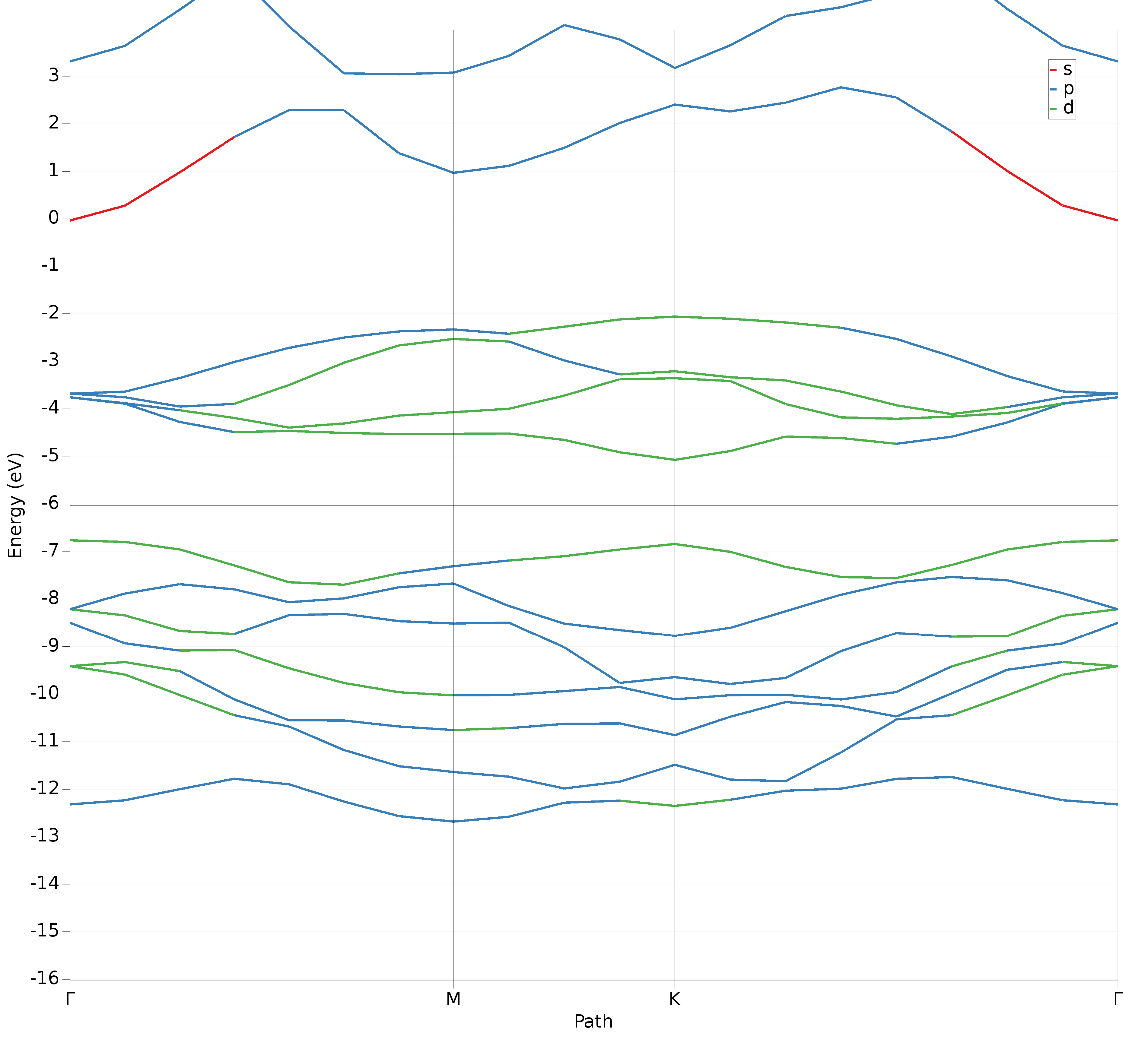
The bands are colored according to the main contribution, also known as ‘fat band analysis’. The band structure will look as follows:
To receive band structure curves that are more smooth, the delta-K parameter of the interpolation can be adjusted.
- 5. Perform a new calculation with the same settings as above6. Select Properties → Band Structure in the panel bar7. In the Interpolation delta-K enter
0.038. Run the calculation and open the Band Structure again

The bands should look much more smooth now. If you zoom in and hover over the bands you should see an indirect band gap from the gamma point to the K point, which is on the edge of the Brillouin zone. (See the indirect band gap at the horizontal black line.)
Electron-hole transport
For semiconductors the shape of the bands near the Fermi level tells you something about how easy the electrons (in the bottom of the conduction band) or holes (in top of the valence band) can move. The inverse of the curvature is called the effective mass of the electron or hole. A small curvature means a large effective mass of the electron or hole, and a large curvature means a large effective mass. To calculate this effective mass:
- Perform a new calculation with the same settings as beforeTick the Effective mass box in Properties → Effective Mass in the panel barRun the calculation. The results will be visible in the Output (.out file)
Tip
See also the BAND tutorial Band Structure and Effective Mass Tensors of Phosphorene
Fix the band gap
The band gap is about 1.7 eV, whereas experimentally it is 1.9 eV (see e.g. Heinz et al. [1] ) We have used the LDA functional, which is known to underestimate the gap. You could try to improve the band gap by using a model potential. For systems that are not crystals, the most convenient choice is the GLLB-SC functional. (XC functional: Model → GLLB-SC) Now the Quasiparticle gap should be a bit higher, since the GLLB-SC includes explicitly the so-called derivative discontinuity.
Applying an electric field
An electric field will reduce the gap significantly. You will need quite strong fields to make the material conducting.
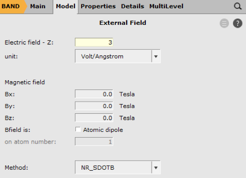
- 1. Switch back to the LDA functional2. In the panel bar, select Model → External field3. In Electric field - Z enter
34. Run the calculation and open the Band Structure
You will find the band character can change a bit at higher fields and you could determine through multiple calculations at what field strength the material will become conducting.
Analyzing the charge
The charge can be analyzed after you applied an electric field.
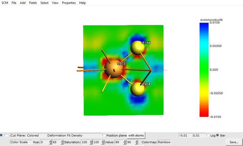
- Select SCM → View in the menu barSelect Add → Cut Plane Colored in the menu barSelect at the bottom Fit density → Fitted deformation densitySelect the atoms with right click and select Atom info → CM5 Charges to show the charges
At a field of 3 Volt/Angstrom and some tweaking (You can change these features by clicking at Cut Plane: Colored → Show Details)
Improving the accuracy
Many aspects influence the results of a calculation. Some are technical, such as the choice of basis set, k-points and integration accuracy; other are theoretical, such as the choice of functional. You can also consider computationally more expensive spin-orbit coupling instead of scalar relativistic. The relativistic effect is small for light atoms and grows with the charge of the nucleus.
The choice of XC functional is not so straightforward. However, to use a GGA is generally better than using the plain LDA. Among the GGAs the PBE functional is a reasonable choice or more modern metaGGAs such as MN15L and SCAN. Finally, the DZ basis set is usually too small, and one should preferably use a TZP one. For the gap (especially when p-electrons are involved) also the spin-orbit might be needed.
References
| [1] | K. Mak, C. Lee, J. Hone, J. Shan, T.F. Heinz Atomically Thin MoS2: A New Direct-Gap Semiconductor, Physical Review Letters 105, 136805 (2010) |