Band Structure and Effective Mass Tensors of Phosphorene
Phosphorene is a 2D material originating from individual sheets of a black Phosphorus crystal. This nanomaterial has experienced a recent spike in interest due to its interesting electronic properties that may one day be relevant in electronic or electromechanical applications.
This tutorial demonstrates how BAND can be used to compute the electronic structure of this material and study it by means of a band structure analysis and Effective Mass tensors. We will compare against the results of the following studies:
L.C. Lew Yan Voon, J. Wang, Y. Zhang, and M. Willatzen Band parameters of phosphorene, J. Phys.: Conf. Ser., (2015).
Y. Cai, G. Zhang, and Y. Zhang Layer-dependent Band Alignment and Work Function of Few-Layer Phosphorene. Sci. Rep. 4, (2015), 6677.
Note
A video variant of this tutorial can also be found under the following link.
Effective Mass Tensors
The concept of effective masses is founded in Newton’s second law
As this relation describes the motion of electrons, the quantities in the above expression gain a slightly different meaning: the acceleration \(\mathbf{a}\) is described as a change of the group velocity \(\mathbf{v}_{g}\), which is in turn given in terms of the dispersion relation \(\mathbf{v}_{g}=\nabla_{\mathbf{k}}\omega(\mathbf{k})\)
The force on the other hand is proportional to the rate of change in the wave vector
which is in turn inserted into the expression, together with the relation \(E(\mathbf{k})=\hbar\omega(\mathbf{k})\):
This leads to a \(3\times3\) tensor relating the force and acceleration vectors with each other:
The meaning of effective mass tensors can be rationalized as follows: in the vacuum, the acceleration of an electron when an electric field is applied is simply given in terms of its rest mass. The acceleration will also follow the direction of the force applied. In a periodic potential however, the motion of an electron can be vastly different from that in the vacuum. In fact this motion strongly depends on the band structure, and may occur in different directions than that of the force applied. The effective mass tensor is exactly the quantity that translates an applied force into the resulting acceleration of the electron.
Also note that the motion of electrons and electron holes typically occurs at the lowest energies, hence at the bottom of the conduction band and the top of the valence band, respectively. By default, these locations in reciprocal space are determined automatically by the engines of the Amsterdam Modelling Suite.
Black Phosphorus and Phosphorene
Black phosphorus is the most stable allotrope of phosphorus at standard conditions and consists of layers. There are only weak bonds between these layers which can therefore be peeled off mechanically. A single of such layers is called Phosphorene, a 2D material which is best described as the Phosphorus analogue of Graphene.
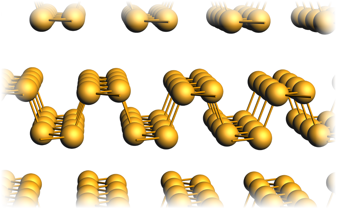
Note the pronounced grooves in each layer along the so-called zig-zag direction. Electrons travelling along this direction are subject to vastly different interactions than when travelling along the orthogonal armchair direction, across the grooves. This naturally leads to very anisotropic electronic properties, which will be examined in this tutorial.
Note that often also multilayer structures are called Phosphorene in the research community, a terminology which we will use also here.
To build phosphorene layers in the GUI, first download the cif file for the symmetrized variant of black phosphorus from corresponding materials project website. Afterwards we import the crystalline structure as follows:
- 1. SCM → Input to open amsinput2. File → Import Coordinates…3. Select the downloaded file P_mp-157_symmetrized.cif
The periodic structure has a unit cell with eight atoms forming two distinct layers.
We then generate the structure of a 4-layer Phosphorene sheet:
- 1. Edit → Crystal → Generate Slab… to open amsinput2. adjust the Miller indices to get the right cutting plane (0, 1, 0)3. Generate Slab… to generate the 4-layer Phosphorene structure4. File → Export Coordinates… → .xyz save as 4LayerPhosphorene.xyz
The remaining 3- to 1-layer structures are then obtained by repeating the above steps followed by selecting and removing all atoms of the lowest, 1, 2, and 3 layers at the bottom, respectively. We also store the structure of the black Phosphorus bulk as we compare its computed properties for it with those of the 1-4 Phosphorene layer structures.
The following periodic structures were optimized with BAND at the PBE/TZP level:
Settings
Once the structures are ready we set the following calculation options for each structure
- 1. File → Import Coordinates to load the structure2. in Main panel: Task → Geometry Optimization →
 3. in Geometry Optimization panel: check the Optimize Lattice checkbox4. Select Optimization method → FIRE.5. return to
 panel: XC functional → libXC.. → 6. under LibXC functional type PBE7. return to panel: Basis set → TZP8. Core → None-. Relativity → None (Do this for compatibility, otherwise results slightly different)9. Numerical Quality → Good and →10. in Numerical Quality panel: Kspace → Good11. in K-space Integration panel: Kspace grid type → Symmetric12. return to panel: check the Calculate band structure checkbox → 13. in Band Structure panel: interpolation delta-K → 0.01 Bohr-114. switch to panel Properties → Effective Mass → check the Effective Mass checkbox
Note
We use the LibXC implementation of PBE as it allows for an analytical calculation of the stress tensor, which renders lattice optimizations significantly faster
Note
These are accurate production-level BAND calculations. Even though the structures provided here are at the PBE/TZP minimum, the computations may require a couple of hours each.
Alternatively, the resulting runscript files for the optimization and effective mass tensor calculation can be downloaded for the individual systems below
- 1. File → Import Coordinates to load either the optimized structures from the previous PBE optimizations or the .xyz files provided above2. in Main panel: Task → Single Point3. XC functional → Range Separated → HSE064. Basis set → TZP5. Core → None6. Numerical Quality → Good →7. in Numerical Quality panel: Kspace → Good →8. in K-space Integration panel: Kspace grid type → Symmetric9. return to panel: check the Calculate band structure checkbox → 10. in Band Structure panel: interpolation delta-K → 0.01 Bohr-111. switch to panel Properties → Effective Mass → check the Effective Mass checkbox
Note
By default the effective mass tensor module of BAND and DFTB automatically determines the top of the valence band and the bottom of the conduction band in the k-space to evaluate the curvature of the band structure.
Note
These are accurate production-level BAND calculations using a hybrid DFT functional. Even though the structures provided here are not optimized, the computations may require a couple of hours each.
Alternatively, the resulting runscript files for the effective mass tensor calculation can be downloaded for the individual systems below
Note that, by default the effective mass tensor module of BAND and DFTB automatically determines the top of the valence band and the bottom of the conduction band in the k-space to evaluate the curvature of the band structure. In some situation it might be needed to fix the k-points manually, which can be done in the Effective Mass panel by entering the k-space coordinates under At K-point.
Hint
To avoid repeatedly entering the same keywords you can (after having entered the desired settings) use the preset functionality: File → Preset → Save as preset…, enter e.g. PBE_TZP_EffMassTensor, and load the template for a different structure with File → Preset → PBE_TZP_EffMassTensor
Hint
If you want to reproduce the numbers presented here there are two issues. First, the relativistic default changed from None to Scalar. For reproducing: Relativity → None . Second, the default optimizer changed from FIRE to Quasi-Newton. For reproducing the result it recommended to simply run Single Point calculations Task → Single Point on the geometries found in Download structures (see above).
Results
Optimized Structures
From the lattice optimization of the different Phosphorene structures and the black Phosphorus crystal, we compare the lattice constants. These values can e.g. be found by
- 1. SCM → Movie to invoke AMSmovie2. Graph → Vector Length → Vector1/2/3
| \(|\mathbf{a}|\) | \(|\mathbf{b}|\) | \(|\mathbf{c}|\) | avg layer distance | |
|---|---|---|---|---|
| 1-Layer | 3.298 Å | 4.687 Å | ||
| 2-Layer | 3.309 Å | 4.630 Å | 5.600 Å | |
| 3-Layer | 3.310 Å | 4.613 Å | 5.607 Å | |
| 4-Layer | 3.311 Å | 4.608 Å | 5.608 Å | |
| Bulk | 3.311 Å | 4.585 Å | 10.989 Å | 5.494 Å |
You can see that the monolayer Phosphorene lattice parameters optimized at the PBE/TZP level agree with the plane wave result of Lew Yan Voon et al.; 3.298 Å vs 3.3 Å and 4.6224 Å vs 4.687 Å, respectively. This agreement can be considered as very good, given the very different numerical approaches used.
From the calculations of the other systems we notice a steady trend in the lattice constants when going from the monolayer to the bulk material; \(|\mathbf{a}|\) increases slightly from 3.298 Å to 3.311 Å, while \(|\mathbf{b}|\) is reduced from 4.687 Å to 4.585 Å. In vertical direction we find the average distance between layers to first increase slightly from the 2- to the 4-layer system, while the corresponding value in the bulk material drops again down by 0.114 Å. It is thus to assume that the interactions between Phosphorene layers only converges after a larger number of layers.
Band Gaps
The band gaps can be retrieved by
- 1. SCM → Output to start AMSoutput2. Properties → Band Gap Info
We obtain the following results
| PBE | HSE | |
|---|---|---|
| 1-Layer | 0.879 eV | 1.540 eV |
| 2-Layer | 0.561 eV | 1.172 eV |
| 3-Layer | 0.397 eV | 0.987 eV |
| 4-Layer | 0.317 eV | 0.896 eV |
| Bulk | 0.107 eV | 0.620 eV |
We find the PBE band gap of 0.879 eV for the Phosphorene monolayer to compare well with the results of Lew Yan Voon et al., 0.912 eV, and Cai et al., ~0.85 eV. As typical for GGA results, these values underestimate the real band gap somewhat. Indeed, the corresponding hybrid DFT result obtained with HSE06 of 1.54 eV matches with the values obtained by Cai et al., ~1.5 eV, and lies within the ballpark of experimental band gaps (1.5-2.0 eV).
We note that the PBE and HSE band gaps obtained for the other Phosphorene systems are slightly higher than the corresponding results of Cai et al. which likely results that these study used a different functional relax the structures.
In further accordance with the literature, we observe decreasing band gaps when going from the monolayer to the bulk material. This change is remarkably strong and indicates that electronic properties like the contact resistance of Phosphorene can be tuned altering the layer thickness. Along with the strongly anisotropic conductivity discussed below, this tunable band gap spurs a tremendous research interest in Phosphorene regarding future electronic applications.
Band Structures
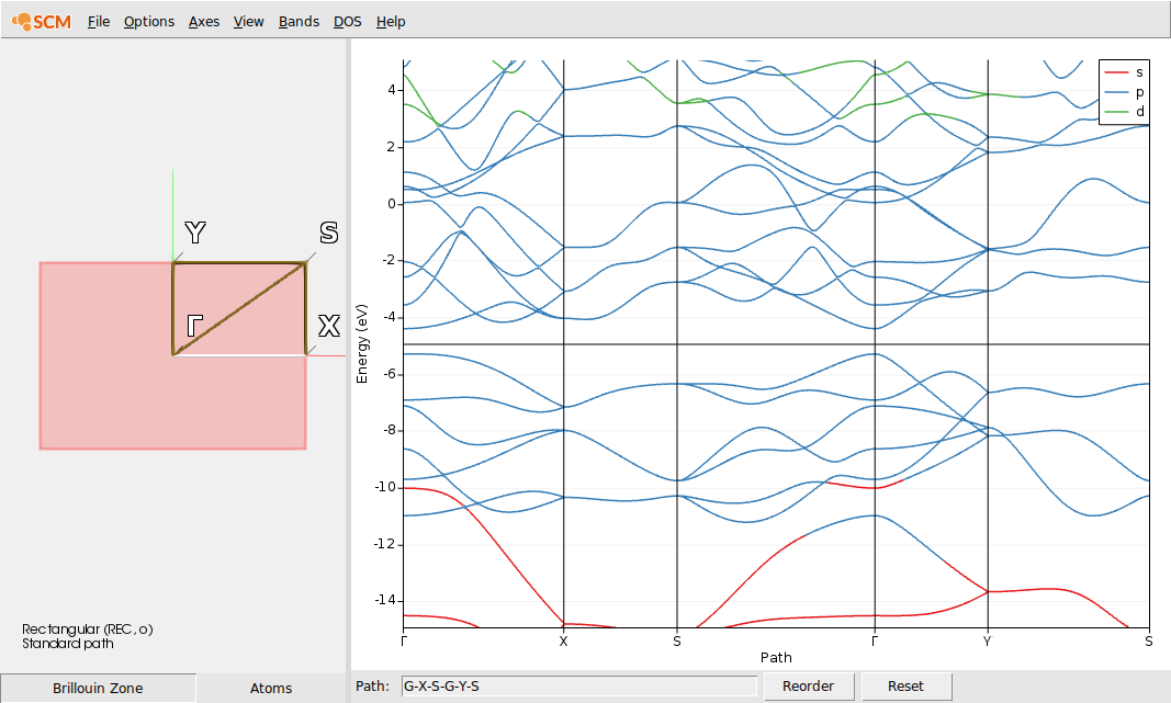
The band structures can be inspected by
- 1. SCM → Band Structure
which opens the AMSbandstructure program and shows the band structure on an autogenerated path
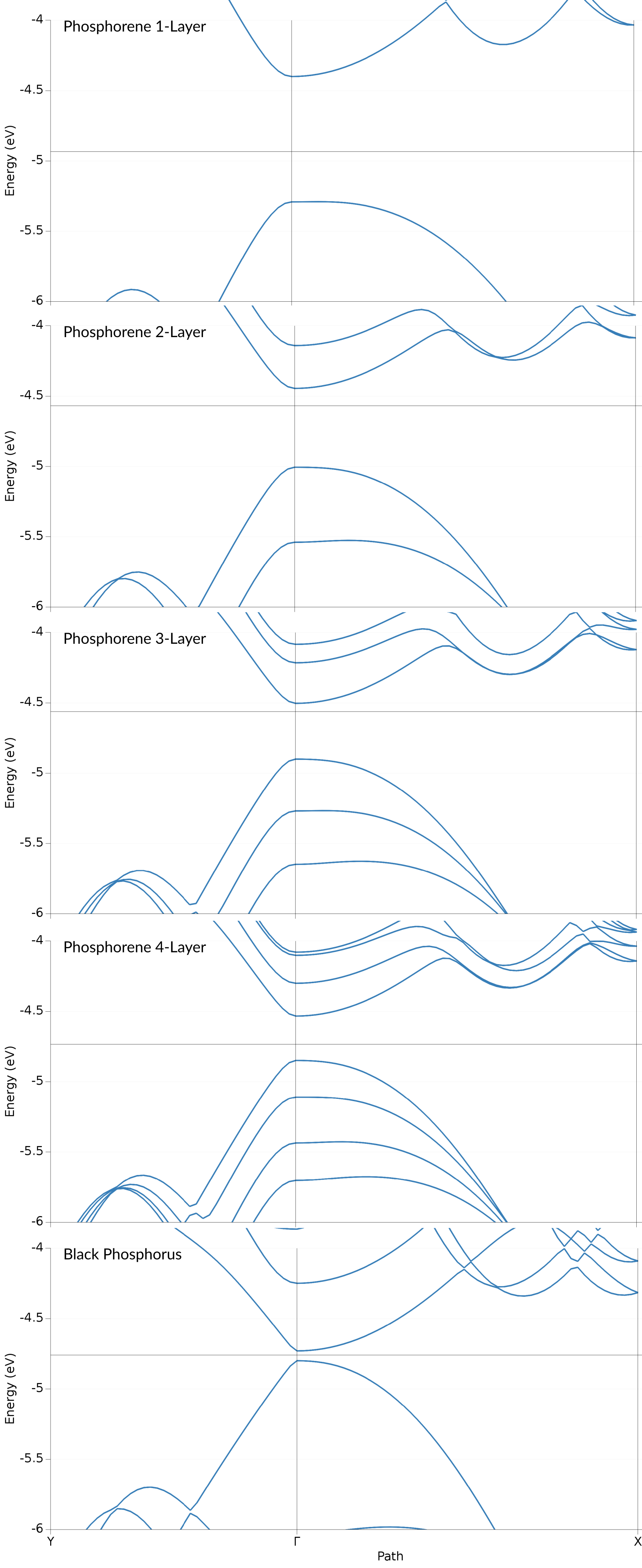
We bring this into the form comparable with the valence band shown by Lew Yan Voon et al. (Figure 2).
Note
The structures used here are rotated by 90° in the XY-plane compared to those of Lew Yan Voon et al. The X and Y indices are thus be interchanged in the discussion below.
- 2. Below the band structure plot Path: → Y-G-X3. Double-click on x-axis to open the Graph options window4. Enter Maximum value → 1.05. Switch to panel Left Y axis6. Enter Minimum value → -6.07. Enter Minimum value → -4.08. Close with OK
For the PBE/TZP results this results in the following
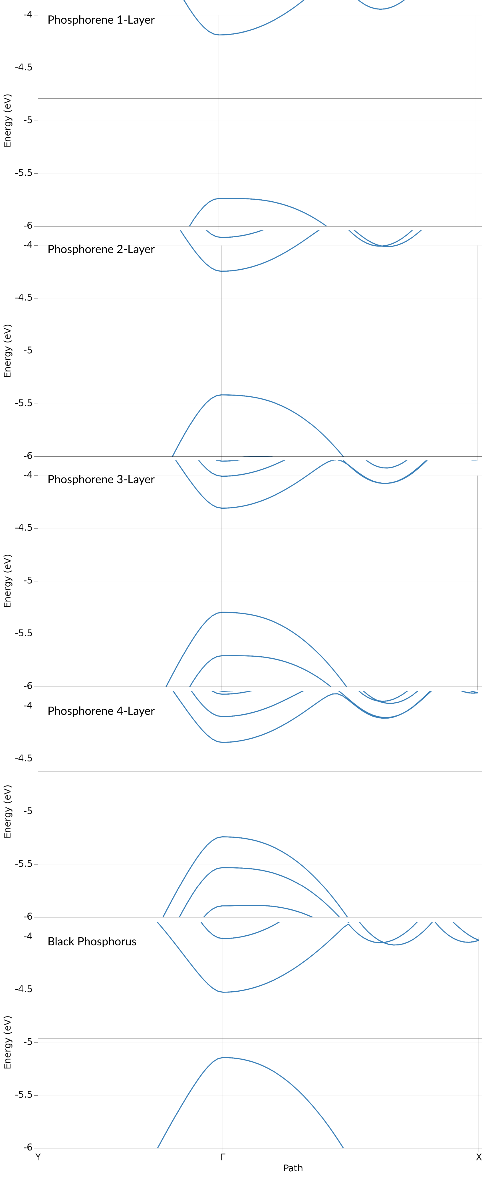
For the HSE/TZP results on PBE structures this results in the following
We find that both, the valence and conduction band, consist of Phosphor p-orbitals. Both of these band also show a clearly anisotropic dispersion: in the \(\Gamma\)-Y (armchair) direction both bands exhibit a steep dispersion. Orthogonal to that, along the \(\Gamma\)-X (zig-zag) direction the bands have a lower curvature. The valence band shows a local maximum slightly shifted away from the \(\Gamma\) point. Both of these features can be found also in the results of Lew Yan Voon et al. (Figure 2), with the local maximum along \(\Gamma\)-X being more pronounced in their case.
The bands obtained form the HSE show a similar result, only with the valence and conduction band being spread further apart, which leads to the aforementioned higher band gap.
Effective Masses
The effective mass tensors are best retrieved via
- 1. SCM → Output2. In the search bar on the bottom: type effective mass3. Use the arrow buttons to scroll to the effective mass tensor output section which looks like the example given below
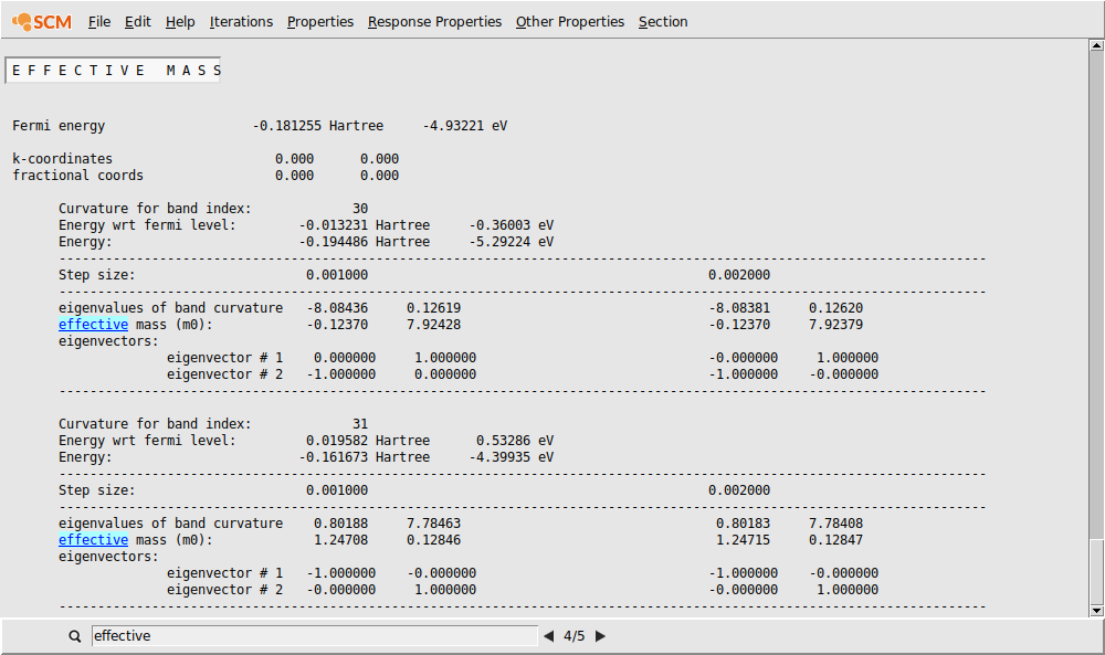
The effective mass tensor block in the output is printed for each band it is applied to (default: valence and conduction band). For each of these bands relevant quantities like energies are listed. This is followed by the curvature of the bands at two different numerical step sizes, which in correct cases gives two matching sets of effective masses. The effective masses are then listed, followed by the corresponding eigenvectors (linewise).
For the computed systems we obtain the following results for conduction (electron masses) and valence band (hole masses). Note, that the hole masses are negative as the bands are concave.
| zig-zag | armchair | |||
|---|---|---|---|---|
| electron | hole | electron | hole | |
| 1-Layer | 1.247 | -2.192 | 0.128 | -0.130 |
| 2-Layer | 1.319 | -7.208 | 0.111 | -0.105 |
| 3-Layer | 1.307 | -3.663 | 0.093 | -0.089 |
| 4-Layer | 1.308 | -2.896 | 0.081 | -0.077 |
| Bulk | 1.364 | -1.663 | 0.023 | -0.023 |
The effective masses computed with PBE for the monolayer system agree well with those reported by Lew Yan Voon et al. The electron mass in zig-zag direction matches almost perfectly (1.240 vs 1.247), while the effective masses in armchair direction are lower than the literature results but still well within acceptable limits. The large effective masses for the electron holes in zig-zag direction are a direct result of the local maximum of the valence band and has been reported to depend very sensitively on numerical parameters used.
The effective masses computed here also reproduce the results of Cai et al.: the masses in zig-zag direction are generally larger than one for both, electrons and holes. While the hole masses exhibit more fluctuations, the electron masses are found to raise from 1.247 (vs 1.23) to about 1.31 for the multilayer systems. The effective masses in armchair direction are significantly lower suggesting a much higher electron mobility. Furthermore, these masses decrease with raising layer thickness, in agreement with Cai et al.
| zig-zag | armchair | |||
|---|---|---|---|---|
| electron | hole | electron | hole | |
| 1-Layer | 1.125 | -2.179 | 0.157 | -0.155 |
| 2-Layer | 1.190 | -3.490 | 0.161 | -0.146 |
| 3-Layer | 1.181 | -2.317 | 0.156 | -0.141 |
| 4-Layer | 1.180 | -1.959 | 0.153 | -0.138 |
| Bulk | 1.165 | -1.208 | 0.134 | -0.121 |
The effective masses from HSE appear slightly lower compared to the PBE results, indicating to a somewhat lower band dispersion which is in line with the tendency of hybrid DFT methods to localize electrons more. With the bilayer Phosphorene system as outlier, we can generally observe the same trends as in the case of the PBE results.